Organic light-emitting device
a light-emitting device and organic compound technology, applied in the direction of discharge tube luminescnet screens, discharge tube/lamp details, electric discharge lamps, etc., can solve the problems of degradation of the hole-transporting layer, insufficient stability of the existing device, and the inability to apply the device to the light-emitting device for emitting green light or blue light, etc., to achieve wide band gap, reduce emission intensity, and high emission efficiency
- Summary
- Abstract
- Description
- Claims
- Application Information
AI Technical Summary
Benefits of technology
Problems solved by technology
Method used
Image
Examples
example 1
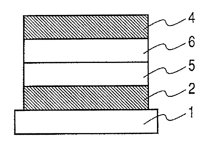
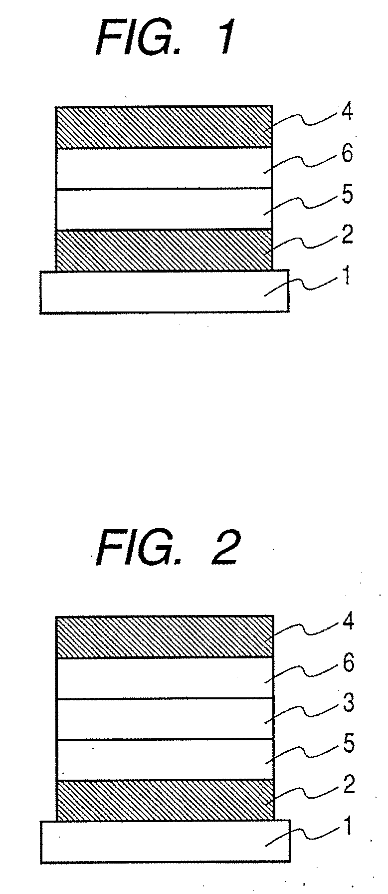
[0075] An organic light-emitting device with a configuration shown in FIG. 2 was produced.
[0076] A transparent conductive support substrate was prepared which had a film of indium tin oxide (ITO) with a thickness of 120 nm as an anode 2 formed on a glass sheet as a substrate 1 by a sputtering method. The transparent conductive support substrate was ultrasonically cleaned sequentially with acetone and isopropyl alcohol (IPA), subsequently cleaned with boiled IPA, was dried, was further cleaned with UV / ozone, and was used.
[0077] A hole-transporting layer 5 was formed by co-evaporation of TFLFL represented by the formula shown below as a main component and Compound 1 represented by the formula shown below as a second component from separate boats. The layer had a concentration of Compound 1 of 3 wt. % and a thickness of 40 nm.
[0078] Next, a light-emitting layer 3 was formed by co-evaporation of Compound 2 represented by the formula shown below as a main component and Compound 3 rep...
example 2
[0096] A light-emitting device was produced by following the same procedure as in Example 1 with the exception that Compound 4 shown below was used as the main component of the light-emitting layer 3; Compound 5 shown below was used as a light-emitting dopant; and ANPD and Compound 6 shown below were used as the main component and second component of the hole-transporting layer 5, respectively.
[0097] When a voltage of 4.5 V was applied to the thus obtained device with the ITO electrode (anode) being used as a positive electrode and the aluminum electrode (cathode) being used as a negative electrode, emission of a blue light derived from Compound 5 and having a maximum emission wavelength of 450 nm with an emission luminance of 300 cd / m2 and an emission efficiency of 2.31 lm / W.
[0098] Furthermore, when a voltage was applied to the device in a nitrogen atmosphere for 100 hours so that the current density was kept at 30 mA / cm2, the device emitted light at a luminance of about 1,100 c...
PUM
 Abstract
Description
Claims
Application Information
 - R&D
- Intellectual Property
- Life Sciences
- Materials
- Tech Scout
- Unparalleled Data Quality
- Higher Quality Content
- 60% Fewer Hallucinations
Browse by: Latest US Patents, China's latest patents, Technical Efficacy Thesaurus, Application Domain, Technology Topic, Popular Technical Reports.
© 2025 PatSnap. All rights reserved.Legal|Privacy policy|Modern Slavery Act Transparency Statement|Sitemap|About US| Contact US: help@patsnap.com


