Multilayer printed board, electronic apparatus, and packaging method
a printed board and electronic equipment technology, applied in the direction of printed element electric connection formation, waveguides, semiconductor/solid-state device details, etc., can solve the problems of insufficient capacitance of capacitors of the currently-available buried capacitance boards, increased dielectric constant of materials, and increased cost of materials whose dielectric constant is improved, so as to improve the character of the capacitive coupling layer
- Summary
- Abstract
- Description
- Claims
- Application Information
AI Technical Summary
Benefits of technology
Problems solved by technology
Method used
Image
Examples
first embodiment
Mode
[0088] Hereinafter, a multilayer printed board according to a first embodiment mode of the present invention will be described with reference to FIG. 1 to FIG. 13.
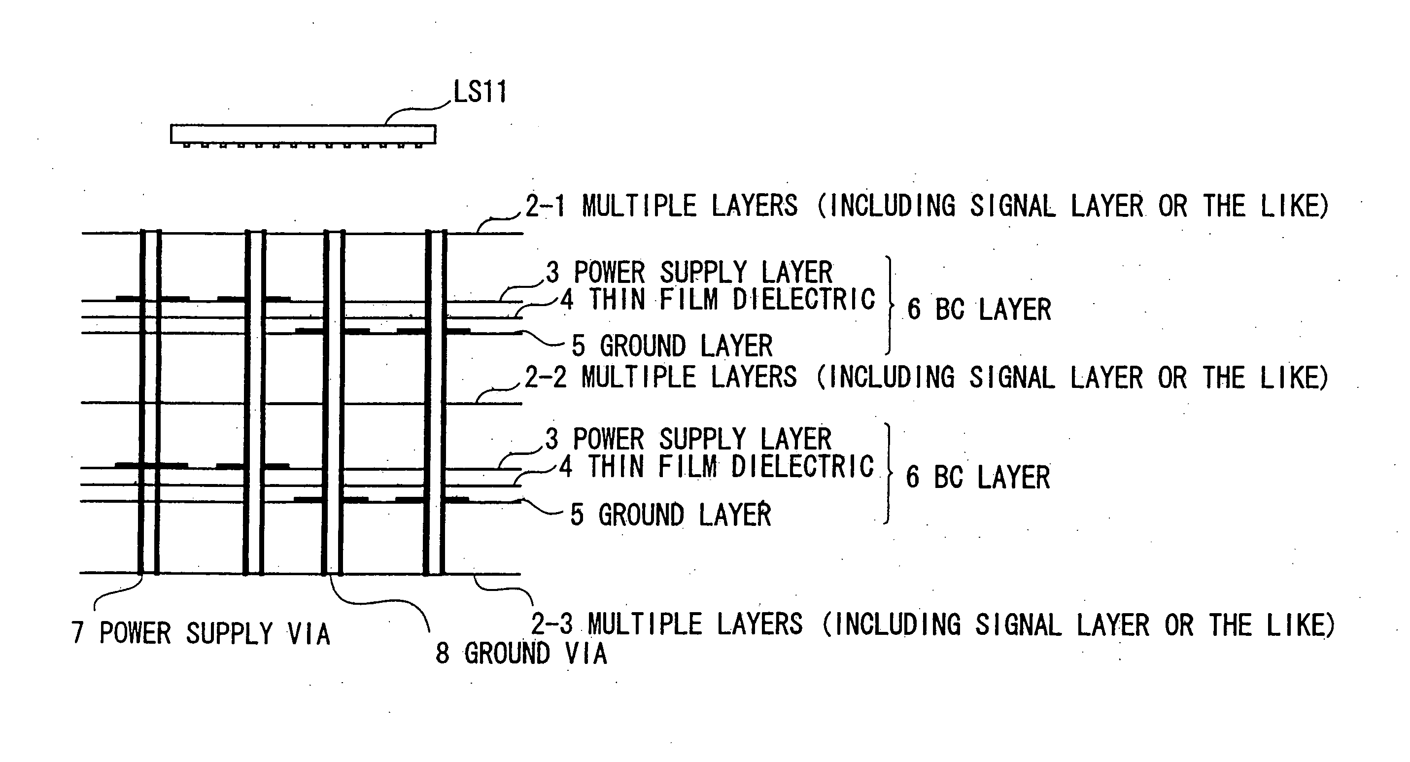
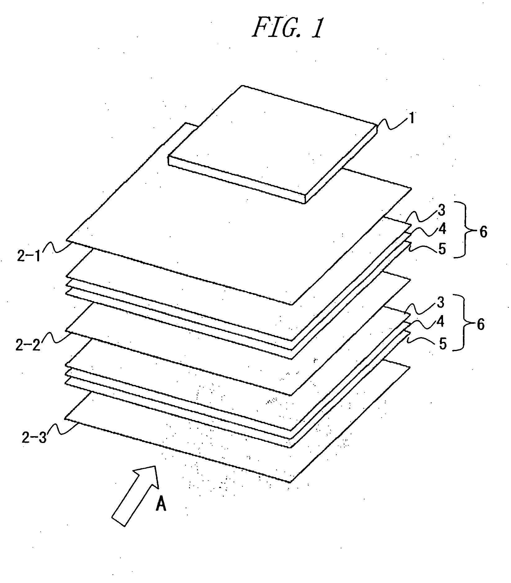
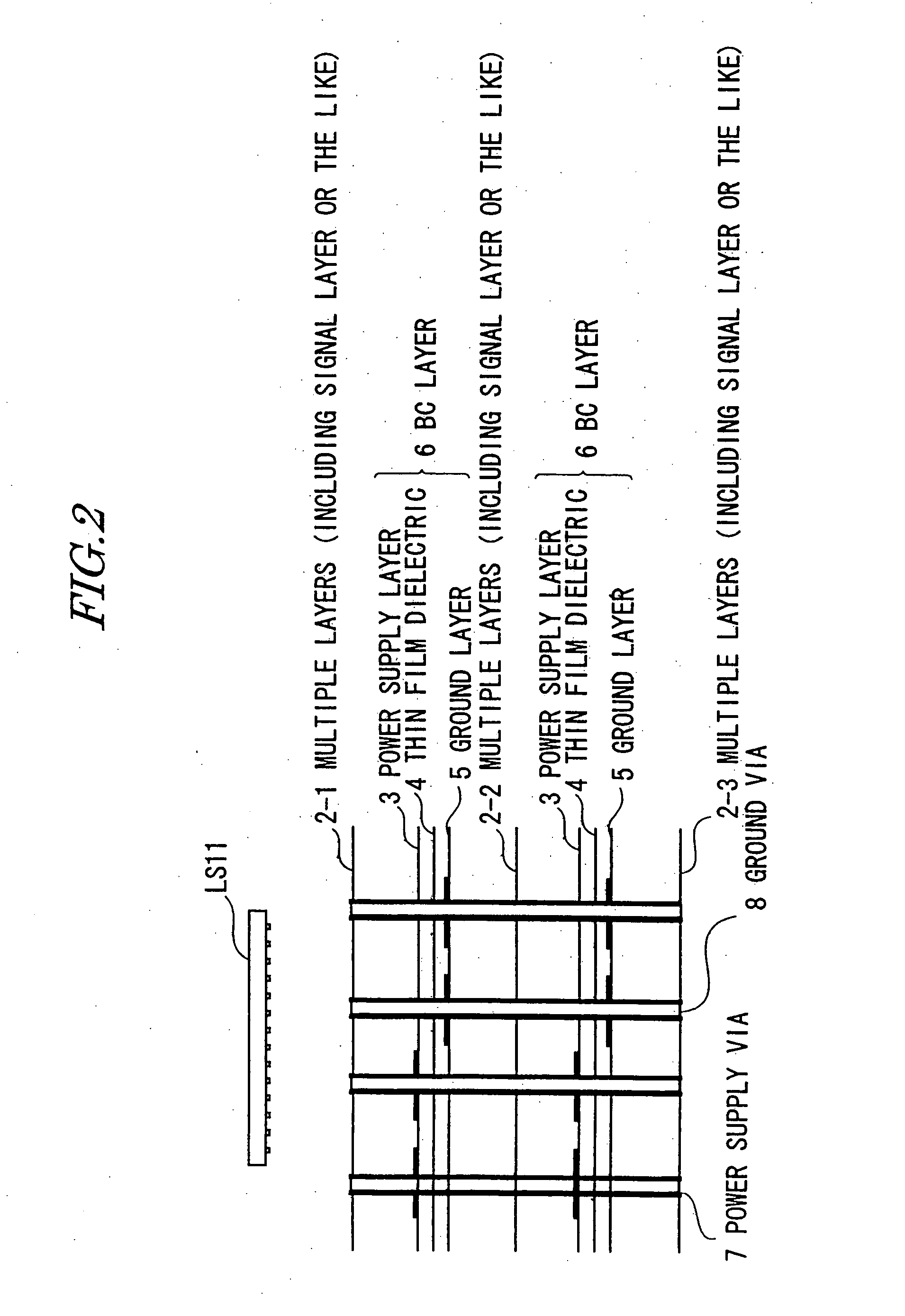
[0089]FIG. 1 is a perspective view showing an example of the multilayer printed board. FIG. 2 is a front view in the case where the multilayer printed board is viewed from a direction indicated by an arrow A in FIG. 1. As shown in FIG. 1 or FIG. 2, the multilayer printed board includes an element such as an LSI 1, printed boards 2-1, 2-2, and 2-3, each of which has a signal layer connected with the element, and BC layers 6 located between the printed boards 2-1 and 2-2 and the printed boards 2-2 and 2-3.
[0090] The printed boards 2-1, 2-2, 2-3, etc. each are composed of a single or plural printed boards. In the case of plural items, they are referred to as multiple layers 2-1, 2-2, 2-3, etc. In general, each of the printed boards 2-1, 2-2, 2-3, etc. includes a conductive layer (this is referred to as the signal layer)...
embodiment 1
[0104]FIG. 3 and FIG. 4 show a structure of a multilayer printed board according to Embodiment 1 of the present invention. In this embodiment, numerical analytical results obtained by calculation of a modeled multilayer printed board are shown. FIG. 3 is a front view showing an analytical model in the case where the multilayer printed board is viewed from the front (for example, the direction indicated by the arrow A in FIG. 1) as in FIG. 2.
[0105] As shown in FIG. 3, the multilayer printed board includes an insulator 2A, a power supply layer 3-1, a thin film dielectric 4-1, a ground layer 5-1, an insulator 2B, a power supply layer 3-2, a thin film dielectric 4-2, a ground layer 5-2, and an insulator 2C. Note that a signal layer is formed on an upper side of the insulator 2A or a lower side of the insulator 2B in an original multilayer printed board. In this embodiment, the influence of the signal layer is not considered for the simplification of the model.
[0106] Each of the insula...
embodiment 2
[0147]FIG. 8 and FIG. 9 show Embodiment 2. In Embodiment 1, the number of power supply vias 7B is made equal to the number of ground vias 8. They are increased from one set (V1G1-1) to five sets (V1G1-5) by one and the impedance characteristic of the BC layers 6 are calculated. In Embodiment 2, a ratio between the number of power supply vias 7B and the number of ground vias 8 is set to 1:2. Such a combination is increased from one set to four sets and the impedance characteristic of the BC layers 6 are calculated. Other structures are identical to those in Embodiment 1.
[0148]FIG. 8 shows the position of the power supply pin of the LSI 1 (power supply via 7A) and the positions of the power supply vias 7B and the ground vias 8 in this embodiment. As shown in FIG. 8, even in any of V1G2-1 to V1G2-4, a pair of ground vias 8 are provided on both sides of each of the power supply vias 7 to make one set.
[0149] In the case of V1G2-1, the one set is provided on the left side of the power s...
PUM
 Abstract
Description
Claims
Application Information
 - R&D
- Intellectual Property
- Life Sciences
- Materials
- Tech Scout
- Unparalleled Data Quality
- Higher Quality Content
- 60% Fewer Hallucinations
Browse by: Latest US Patents, China's latest patents, Technical Efficacy Thesaurus, Application Domain, Technology Topic, Popular Technical Reports.
© 2025 PatSnap. All rights reserved.Legal|Privacy policy|Modern Slavery Act Transparency Statement|Sitemap|About US| Contact US: help@patsnap.com


