Charged particle beam apparatus
a beam apparatus and charge technology, applied in the field of chargeable particle beam apparatus, can solve problems such as pits in the substrate, and achieve the effect of suppressing defects and inhibiting sample contamination
- Summary
- Abstract
- Description
- Claims
- Application Information
AI Technical Summary
Benefits of technology
Problems solved by technology
Method used
Image
Examples
example 1
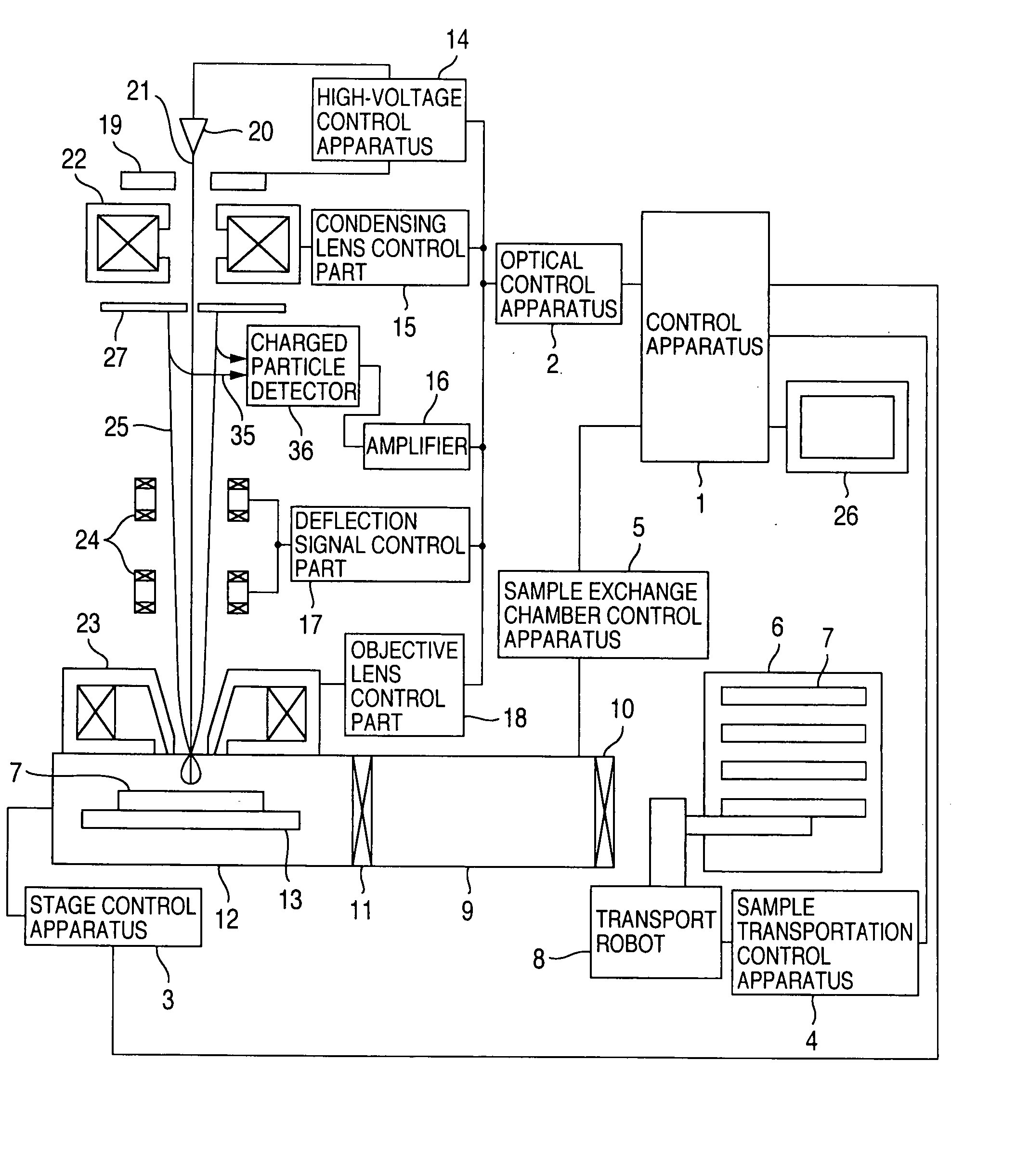
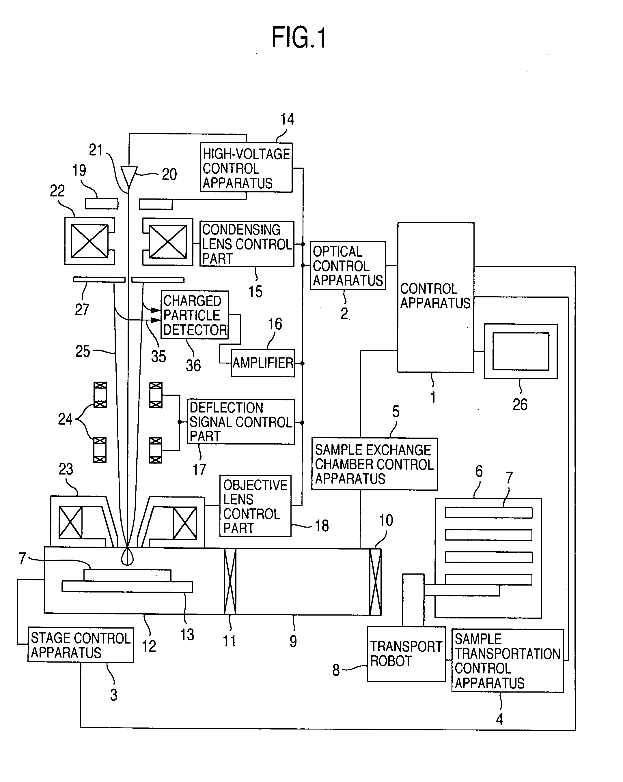
[0019]FIG. 1 is a view for describing an outline of a scanning electron microscope that illustrates one example of this invention. A control apparatus 1 controls an optical control apparatus 2, a stage control apparatus 3, a sample transportation control apparatus 4 and a sample exchange chamber control apparatus 5 on the basis of an accelerating voltage, sample (semiconductor device) information, measurement location information, wafer cassette information and the like input by an operator from a user interface (not shown in the figure).
[0020] Upon receiving an instruction from the control apparatus 1, the sample transportation control apparatus 4 controls a transport robot 8 so as to transport an arbitrary wafer 7 from a wafer cassette 6 to a predetermined location in a load lock chamber 9 (sample exchange chamber). The sample exchange chamber control apparatus 5 carries out control so as to open and close gate valves 10 and 11 in response to movement of the wafer 7 into and out ...
example 2
[0048] The embodiment described above relates to a specific technique that prevents impurities from adhering to a sample as well as the configuration of the apparatus. In contrast, hereunder a description is provided that relates to a method and apparatus that enable the performance of appropriate measures such as washing even in a case in which some kind of impurity adhered to a sample, by accurately recognizing that situation.
[0049]FIG. 5 is a view illustrating a case in which a detection apparatus for detecting substances that adhered to or that may adhere to a sample was provided in a sample chamber of an electron microscope. FIG. 5 is an enlarged view of the load lock chamber 9 and the sample chamber 12 of FIG. 1. In the sample chamber 12 is provided a vacuum pump 101 for evacuating the inside of the sample chamber 12 through an evacuation pipe 102.
[0050] To the evacuation pipe 100 is connected a quadrupole mass spectrometer 102 for analyzing components of trace amounts of ga...
example 3
[0057] In this embodiment, another example of installing in a sample chamber of an electron microscope a detection apparatus for detecting substances that adhered to or that may adhere to a sample is described using FIG. 6.
[0058]FIG. 6 illustrates an example in which a light source 201 and a detector 202 of an infrared spectrophotometer were installed in a sample chamber 12 of an electron microscope. The light source 201 and the detector 202 are disposed in a condition such that there is no obstruction in the space between them, and such that it is possible to detect the state in the area between the light source 201 and the detector 202 when gas is generated inside the sample chamber 12. A configuration is adopted whereby an analysis result of the infrared spectrophotometer is stored on a storage medium within the control apparatus 1 and displayed on the display apparatus 26.
[0059] The configuration is such that several kinds of substances that may have an effect on a semiconduct...
PUM
 Abstract
Description
Claims
Application Information
 - R&D
- Intellectual Property
- Life Sciences
- Materials
- Tech Scout
- Unparalleled Data Quality
- Higher Quality Content
- 60% Fewer Hallucinations
Browse by: Latest US Patents, China's latest patents, Technical Efficacy Thesaurus, Application Domain, Technology Topic, Popular Technical Reports.
© 2025 PatSnap. All rights reserved.Legal|Privacy policy|Modern Slavery Act Transparency Statement|Sitemap|About US| Contact US: help@patsnap.com


