
Method and apparatus for testing a TFT array for a liquid crystal panel

Inactive Publication Date: 2007-08-02
AGILENT TECH INC
View PDF0 Cites 7 Cited by
  • Summary
  • Abstract
  • Description
  • Claims
  • Application Information

AI Technical Summary

Benefits of technology

[0010]That is, it is possible to detect the dynamic electrical properties of a liquid crystal element by checking to what extent a liquid crystal element has accumulated a charge immediately after a voltage that will apply a field in the opposite direction has been applied to a liquid crystal to which a field in a predetermined direction has been pre-applied. A liquid crystal element having a poor response from groups of molecules will also have a poor electrical response. Therefore, it is possible to detect defective pixels with a poor response from groups of molecules by detecting the electrical properties. It is possible to prevent testing-related deterioration of the liquid crystal element by bringing the voltage that is applied to supply the charge that will be detected to the voltage that is of the opposite polarity, but is of the same absolute value as the preapplied voltage.
[0013]The present disclosure makes it possible to provide a method with which it is possible to precisely check for defects based on the dynamic properties of a liquid crystal display panel, etc.

Problems solved by technology

A liquid crystal element having a poor response from groups of molecules will also have a poor electrical response.
In general, a liquid crystal element having a poor response from groups of molecules will also have a poor electrical response.

Method used


Image

  • Method and apparatus for testing a TFT array for a liquid crystal panel
  • Method and apparatus for testing a TFT array for a liquid crystal panel
  • Method and apparatus for testing a TFT array for a liquid crystal panel

Examples


Embodiment Construction

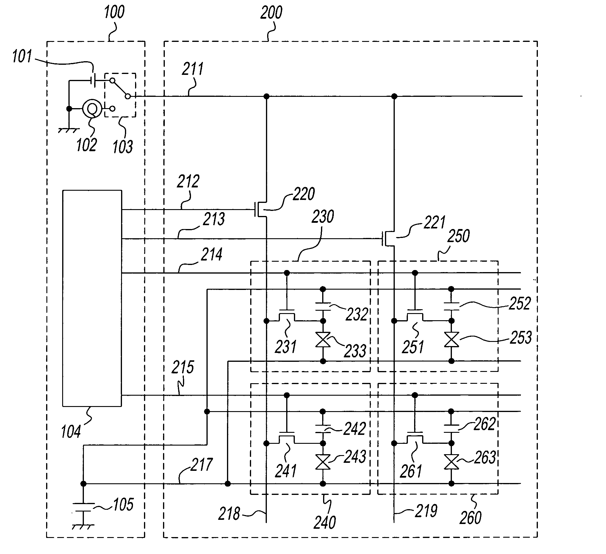
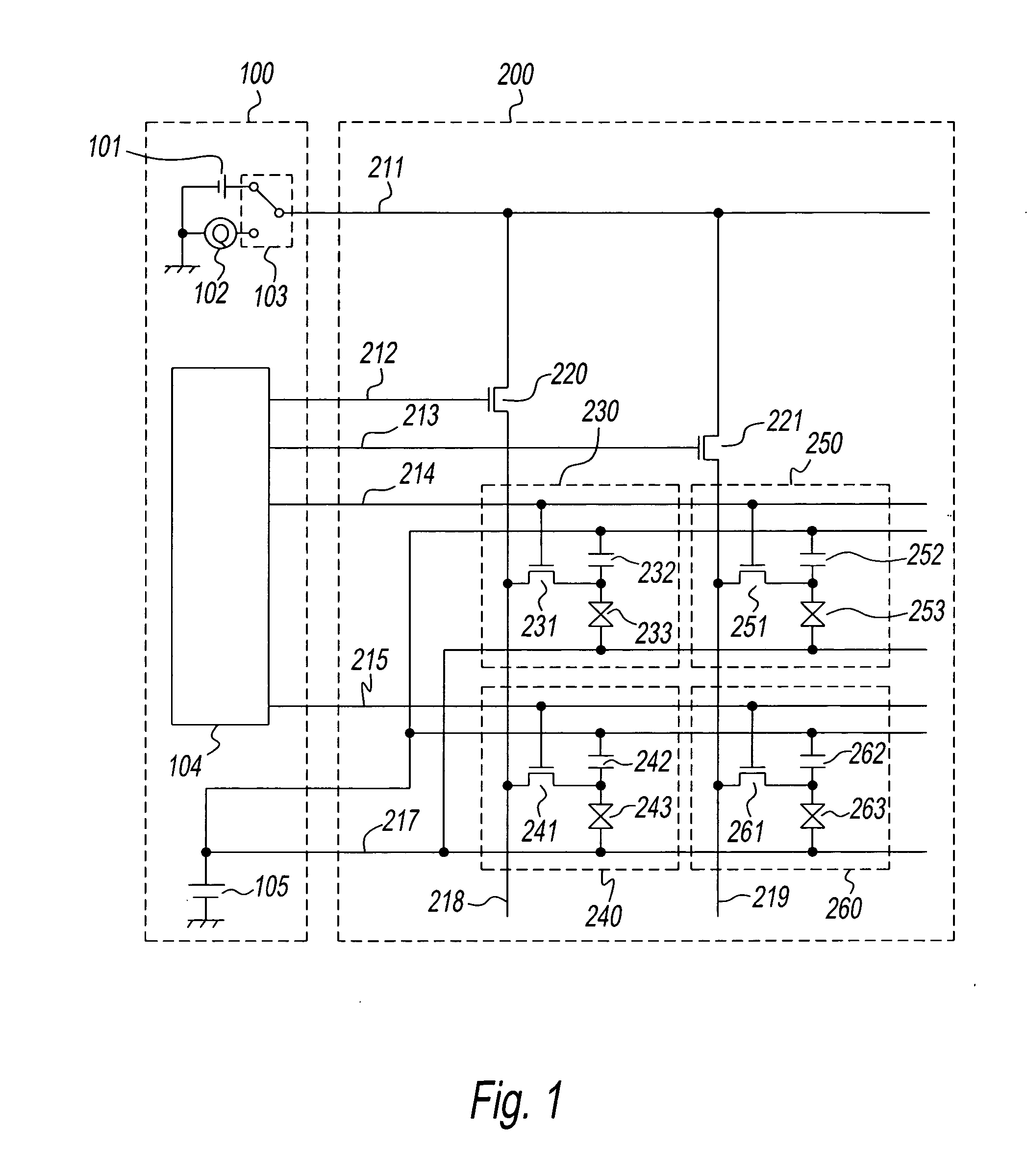
[0018]A typical example of the present disclosure will be described while referring to the drawings. FIG. 1 is a drawing of a testing apparatus 100 of the present disclosure connected to the device under test, a liquid crystal display panel 200.

[0019]Liquid crystal display panel 200 comprises control lines 212, 213, 214, and 215 for selecting pixels, signal lines 218 and 219 that intersect each of the control lines and transmit signals that control the status of the pixels, a transistor 220 for controlling the connection status between a signal input line 211 and signal line 218 from the outside based on the input of control line 212, a transistor 221 that controls the connection status between signal input line 211 and signal line 219 based on the input of control line 213, pixels (230, 240, etc) disposed where the control lines and signal lines intersect, and a common line 217 for applying a reference potential to pixel holding capacitors (232, 242, etc.) and liquid crystal elemen...


PUM


Abstract

A method for testing a liquid crystal display panel wherein there are, disposed in matrix form, pixels comprising liquid crystal elements in which a liquid crystal material is sealed between opposing electrodes, this method for testing a liquid crystal display panel being characterized in that it comprises a first charging step for applying a first voltage between the opposing electrodes of the liquid crystal element of the pixel under test; a second charging step for applying a second voltage of the opposite polarity of the first voltage between the opposing electrodes of the liquid crystal element of the pixel under test; and a measuring step for discharging the charge that has accumulated in the electrodes of the liquid crystal element of the pixel under test after the second charging step, and measuring the amount of charge discharged.

Description

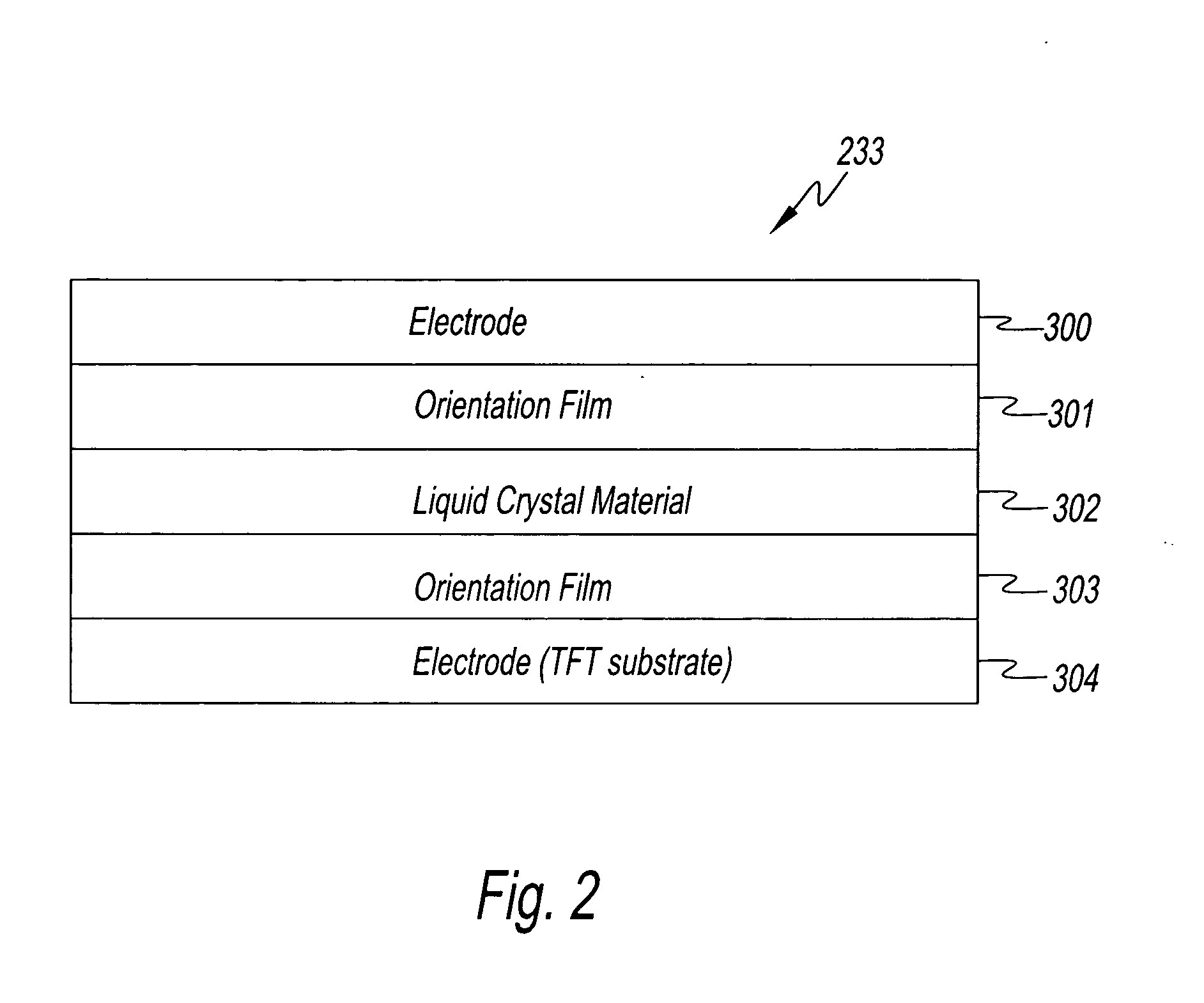
1. FIELD OF THE INVENTION[0001]The present disclosure relates to a manufacturing method and a testing method for a display panel, as well as an apparatus for testing a display panel, and in particular, to a method for manufacturing a liquid crystal display panel in which liquid crystals are sealed.2. DISCUSSION OF THE BACKGROUND ART[0002]The most popular displays that use liquid crystal materials comprise a backlight as the light source, a deflection filter through which passes only light of a constant polarization; and color filters that create the three primary colors. Of these, the general structure of the display panel is such that liquid crystal elements are disposed on an active matrix substrate wherein transistors, a holding capacitor, and other elements are formed for each pixel on a glass sheet or other substrate.[0003]FIG. 2 shows the structure of a liquid crystal element 233 of a typical liquid crystal panel. Liquid crystal element 233 comprises a liquid crystal material ...

Claims


Application Information

Patent Timeline
IPC IPC(8): G01R31/00
CPCG09G3/3648G09G3/006
Inventor MIYAKE, YASUHIRO
Owner AGILENT TECH INC
Learn More