High-throughput printing of chalcogen layer
a chalcogen layer, high-throughput technology, applied in the field of solar cells, can solve the problems of poor surface coverage, difficult and difficult to use traditional vacuum-based deposition process to achieve precise stoichiometric composition over relatively large substrate area
- Summary
- Abstract
- Description
- Claims
- Application Information
AI Technical Summary
Benefits of technology
Problems solved by technology
Method used
Image
Examples
first embodiment
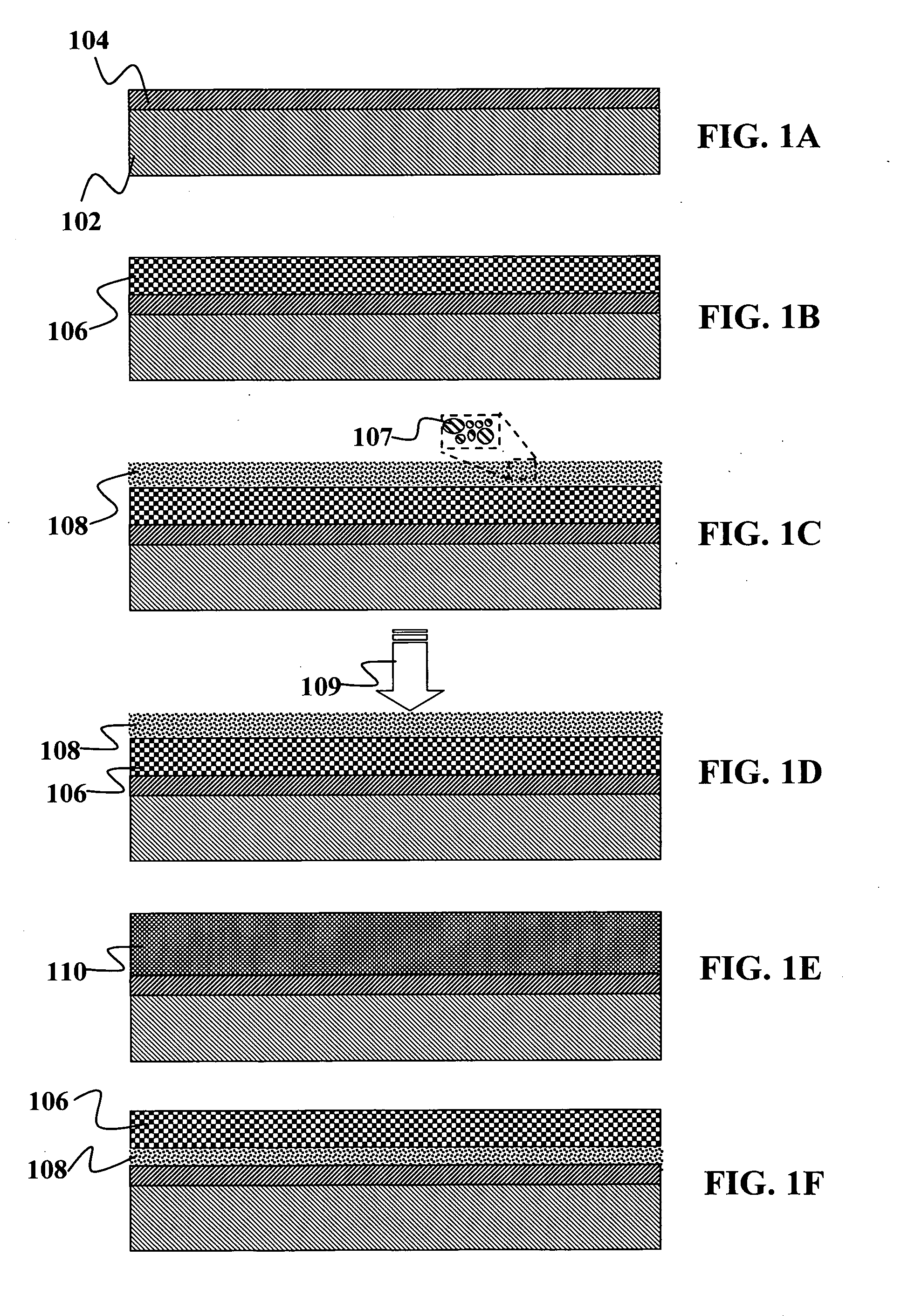
[0033] According to the present invention, the compound layer may include one or more group IB elements and two or more different group IIIA elements as shown in FIGS. 1A-1E.
[0034] The absorber layer may be formed on a substrate 102, as shown in FIG. 1A. By way of the example, the substrate 102 may be made of a metal such as, but not limited to, aluminum. Depending on the material of the substrate 102, it may be useful to coat a surface of the substrate with a contact layer 104 to promote electrical contact between the substrate 102 and the absorber layer that is to be formed on it. For example, where the substrate 102 is made of aluminum the contact layer 104 may be a layer of molybdenum. For the purposes of the present discussion, the contact layer 104 may be regarded as being part of the substrate. As such, any discussion of forming or disposing a material or layer of material on the substrate 102 includes disposing or forming such material or layer on the contact layer 104, if o...
second embodiment
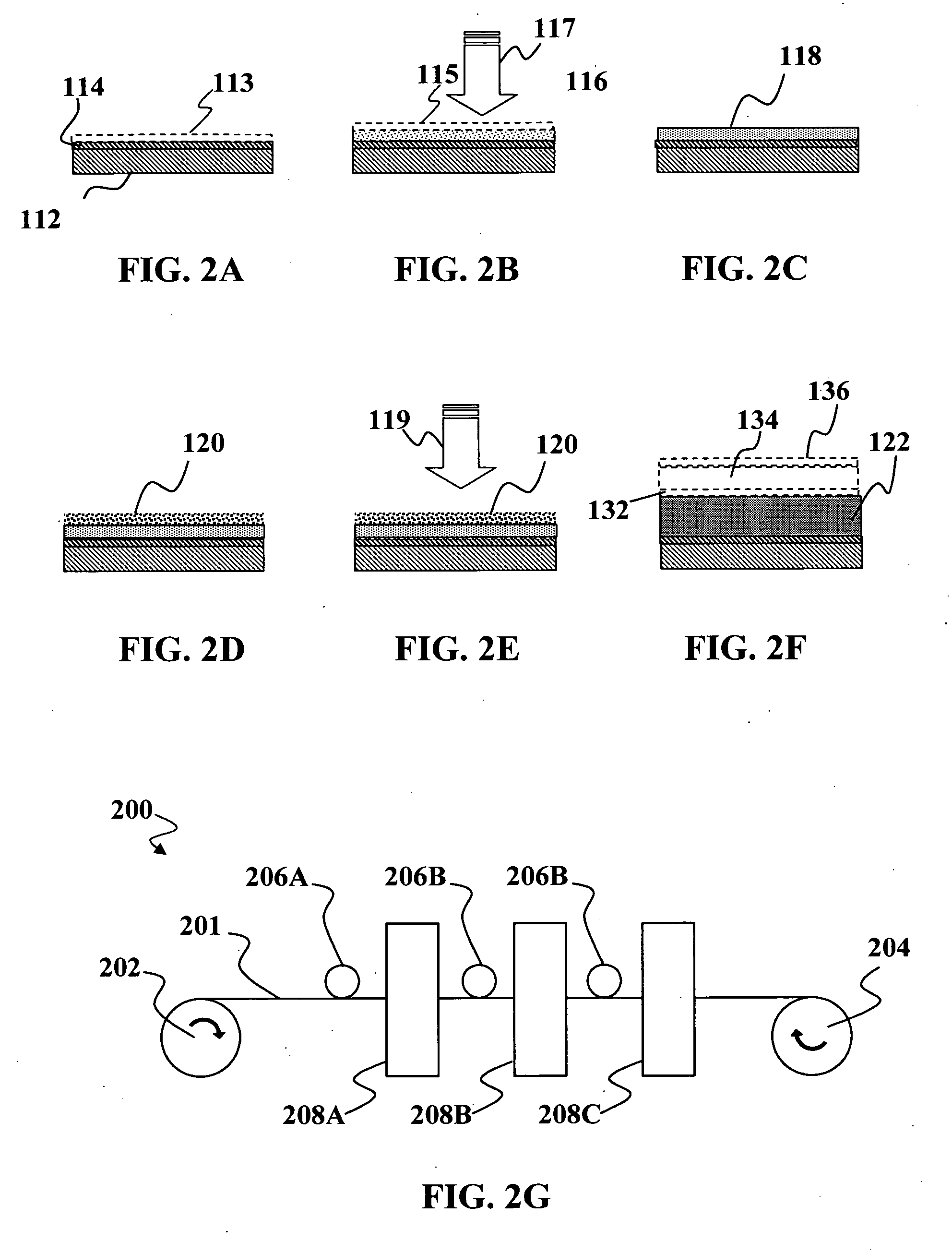
[0059] According to the present invention, the compound layer may include one or more group IB elements and one or more group IIIA elements. Fabrication may proceed as illustrated in FIGS. 2A-2F. The absorber layer may be formed on a substrate 112, as shown in FIG. 2A. A surface of the substrate 112, may be coated with a contact layer 114 to promote electrical contact between the substrate 112 and the absorber layer that is to be formed on it. By way of example, an aluminum substrate 112 may be coated with a contact layer 114 of molybdenum. As discussed above, forming or disposing a material or layer of material on the substrate 112 includes disposing or forming such material or layer on the contact layer 114, if one is used. Optionally, it should also be understood that a layer 115 may also be formed on top of contact layer 114 and / or directly on substrate 112. This layer may be solution coated, evaporated, and / or deposited using vacuum based techniques. Although not limited to the...
PUM
| Property | Measurement | Unit |
|---|---|---|
| Temperature | aaaaa | aaaaa |
| Temperature | aaaaa | aaaaa |
| Temperature | aaaaa | aaaaa |
Abstract
Description
Claims
Application Information
 - R&D
- Intellectual Property
- Life Sciences
- Materials
- Tech Scout
- Unparalleled Data Quality
- Higher Quality Content
- 60% Fewer Hallucinations
Browse by: Latest US Patents, China's latest patents, Technical Efficacy Thesaurus, Application Domain, Technology Topic, Popular Technical Reports.
© 2025 PatSnap. All rights reserved.Legal|Privacy policy|Modern Slavery Act Transparency Statement|Sitemap|About US| Contact US: help@patsnap.com


