Process to integrate fabrication of bipolar devices into a CMOS process flow

a technology process flow, which is applied in the direction of transistors, semiconductor devices, electrical equipment, etc., can solve the problems of increasing the stack height of bipolar junction transistor material layers, affecting the effect of bipolar junction transistor device fabrication efficiency, and affecting the ability of bipolar junction transistor material and material layers to be fabricated. to form the required structural shapes for the base and/or the emitter,

Inactive Publication Date: 2007-07-12
AGERE SYST INC
View PDF6 Cites 4 Cited by
  • Summary
  • Abstract
  • Description
  • Claims
  • Application Information

AI Technical Summary

Problems solved by technology

Erosion of exposed surface layers of the bipolar junction transistor structure during etching to form the MOSFET gate spacers is a known disadvantage of the above-described approach for integrating the bipolar junction transistor and CMOS process flows.
However, this technique increases the stack height of the bipolar junction transistor material layers.
Also, etching of the thicker polysilicon layers, to form the required structural shapes for the base and / or the emitter is more difficult.
Properly filling an emitter window in the base polysilicon layer (for forming the emitter region) is more difficult as the thickness of the base polysilicon layer increases.
According to another known prior art technique, bipolar junction transistor surface layer erosion is limited by careful control of the MOSFET gate spacer etch process, but this technique adds cost to the fabrication process.
Since the final thickness of the polysilicon layer cannot be fully controlled, due to erosion during gate spacer etch, the resistance of these polysilicon resistors may not be within a specified tolerance.

Method used


Image

  • Process to integrate fabrication of bipolar devices into a CMOS process flow
  • Process to integrate fabrication of bipolar devices into a CMOS process flow
  • Process to integrate fabrication of bipolar devices into a CMOS process flow

Examples


Embodiment Construction

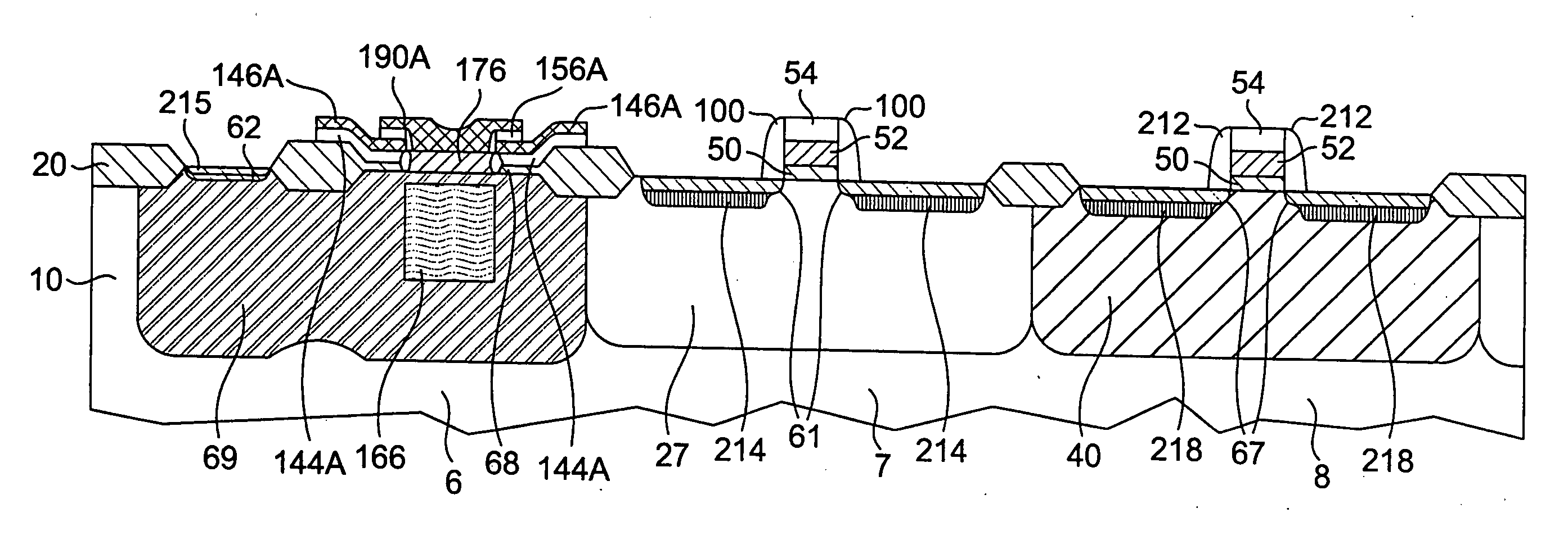
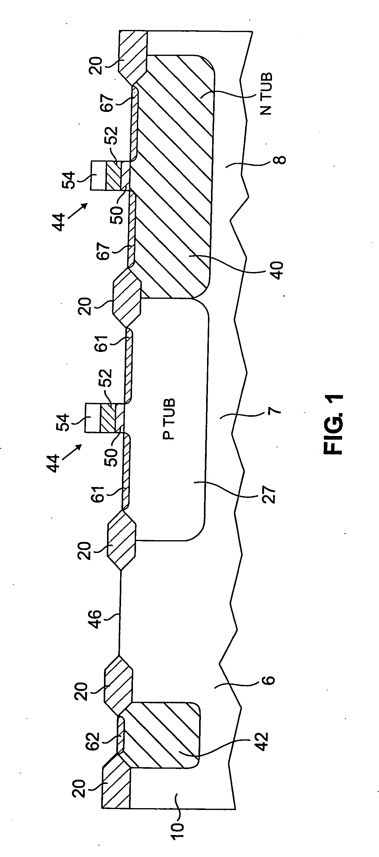
[0021] Before describing in detail the particular method and apparatus for forming bipolar junction transistors and CMOS devices on a semiconductor substrate according to a BiCMOS process flow, it should be observed that the present invention resides primarily in a novel and non-obvious combination of elements and process steps. So as not to obscure the disclosure with details that will be readily apparent to those skilled in the art, certain conventional elements and steps have been presented with lesser detail, while the drawings and the specification describe in greater detail other elements and steps pertinent to understanding the invention. The illustrated process steps are exemplary, as one skilled in the art recognizes that certain independent steps illustrated below may be combined and certain steps may be separated into individual sub-steps to accommodate individual process variations.

[0022] A process sequence for forming single-layer polysilicon bipolar junction transisto...


PUM


Abstract

A BiCMOS method for forming bipolar junction transistors and CMOS devices in a substrate. To avoid erosion of the bipolar junction transistor material layers, gate spacers for the CMOS devices are formed while a bipolar junction transistor photoresist layer is in place. The photoresist layer is used for etching the emitter polysilicon layer (for single polysilicon layer bipolar junction transistors) or for etching the base polysilicon layer (for double polysilicon layer bipolar junction transistors) prior to gate spacer etch.

Description

RELATED APPLICATION [0001] This application is a continuation of U.S. patent application Ser. No. 11 / 237,634 (Chen 18-12-2-11-1), filed Sep. 28, 2005, the contents of which are incorporated herein by reference in their entirety.FIELD OF THE INVENTION [0002] This invention relates generally to fabrication of complementary metal oxide semiconductor field effect transistor devices (CMOS), and more specifically, to fabrication of bipolar junction transistor devices (BJT) into a CMOS fabrication process flow. BACKGROUND OF THE INVENTION [0003] Integrated circuits typically comprise semiconductor devices, such as bipolar junction transistors (BJTS) and metal-oxide semiconductor field effect transistors (MOSFETS) formed in doped regions within a semiconductor layer. Overlying levels of interconnect, formed in dielectric layers, electrically connect the doped regions to form circuits. Conductive vias, also disposed in the dielectric layers, connect conductive runners or traces in different ...

Claims


Application Information

Patent Timeline
Patent Type & Authority Applications(United States)
IPC IPC(8): H01L21/8234H01L21/8238H01L21/8249H01L21/302
CPCH01L21/8249H01L29/66287H01L27/0623
Inventor KERR, DANIEL CHARLESPATNAIK, MAMATAPITA, MARIORAGHAVAN, VENKATCHEN, ALAN SANGONE
Owner AGERE SYST INC
Why Eureka
Try Eureka