
Laser processing apparatus and laser processing process

a laser processing and laser technology, applied in the field of laser processing equipment, can solve the problems of vibration of samples, no technology for reducing malfunction and minute displacement of samples during laser beam irradiation, and no technology for easily irradiating laser beam to the desired portion

Inactive Publication Date: 2007-06-21
SEMICON ENERGY LAB CO LTD
View PDF93 Cites 10 Cited by
  • Summary
  • Abstract
  • Description
  • Claims
  • Application Information

AI Technical Summary

Benefits of technology

The present invention provides a laser annealing process with novel conditions that can produce consistent results. Additionally, the invention includes a laser processing apparatus with a structure that prevents vibration transfer to the laser apparatus. The invention also provides an optimal method for sample alignment. The invention involves activating thin films containing silicon as the main constituent by laser annealing. The process involves irradiating a short wavelength laser beam (400 nm or less in wavelength) while taking into consideration the light transmittance of the film.

Problems solved by technology

Researchers of laboratory scale have been conducted to present, however, many problems concerning the application of laser processing technology to mass production have been left out of consideration.
For instance, no technology for reducing malfunction and minute displacement of the sample during the laser beam irradiation nor technology for easily irradiating the laser beam to the desired portion has been developed to present.
This inevitably vibrates the sample, and the stage vibration is transferred to the laser apparatus.
However, no drastic solution for such a problem has been proposed to present.
Moreover, no profound consideration has been given to the method of sample alignment in using stripe-emitting lasers
Furthermore, no sufficient study on the conditions for laser annealing has been made so far.
Accordingly, it has been generally believed that a laser annealing technology is of no practical use due to the lack of reproducibility and stability.

Method used


Image

  • Laser processing apparatus and laser processing process
  • Laser processing apparatus and laser processing process
  • Laser processing apparatus and laser processing process

Examples


example 1

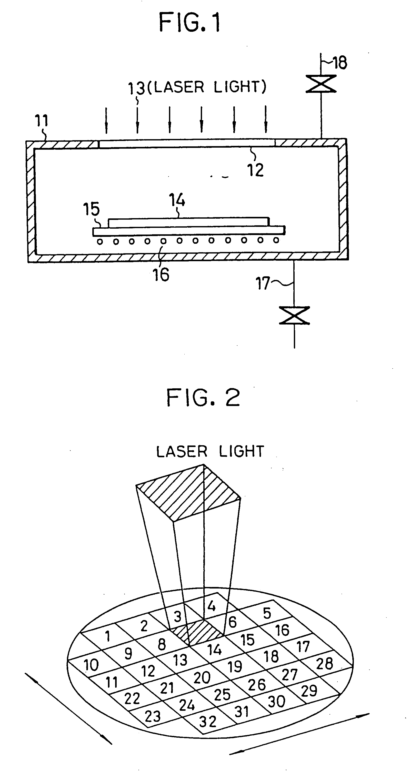
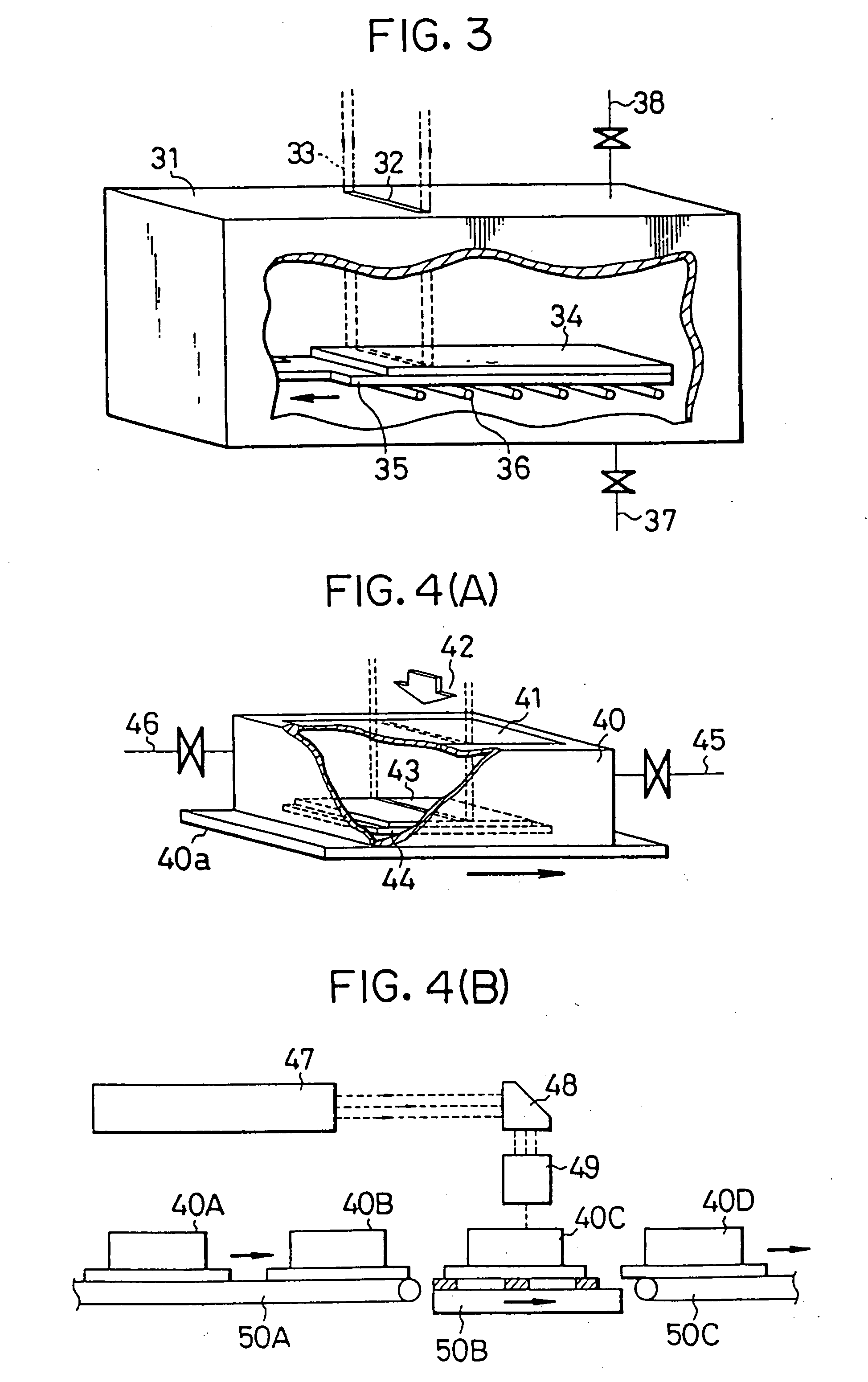
[0044] Referring to FIG. 3, an apparatus for doping process according to the present invention is described below. The apparatus comprises a chamber 31 equipped with a slit-shaped window 32 made of anhydrous quartz glass. A laser beam is irradiated through this window and shaped to have a slit-like cross section, e.g., a rectangular shape 10 mm×300 mm in area. The position of the laser beam is fixed. The chamber also comprises an evacuation system 37, a gas system 38 for introducing a passivation gas. A sample 34 is mounted on a sample holder 35 placed inside the chamber, and is heated by an infrared lamp 36 which functions as a heater provided under the sample holder. The sample holder is movable, and is moved in accordance with the laser shots.

[0045] When a mechanism for moving the sample is assembled inside the chamber as in this example, misalignment occurs due to the thermal expansion of the sample holder being heated by the heater. Thus, strict control of the temperature is r...

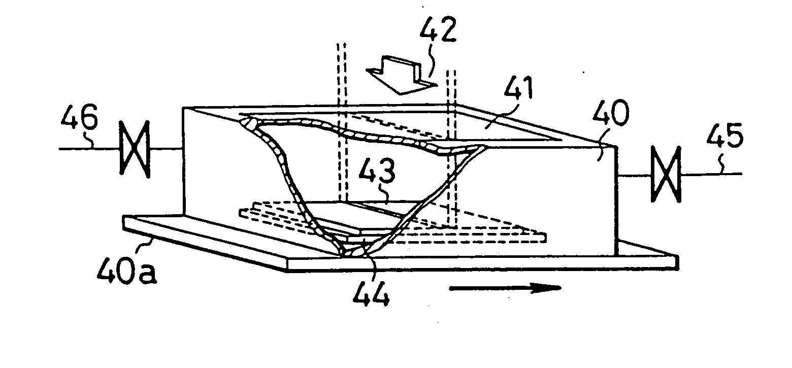
example 2

[0046] Referring to FIG. 4(A), an apparatus for doping process according to the present invention is described below. The apparatus comprises a chamber 40 provided with a window 41 made of anhydrous quartz glass. This window covers the entire area of a sample 43, and it differs in this point from that of the apparatus described in Example 1. An evacuation system 45 and a gas system 46 for introducing the passivation gas are also connected to the chamber. A sample 43 is mounted on a sample holder 44 fixed inside the chamber, and the sample holder is equipped with a built-in heater. A table 40a is provided to the lower part of the chamber so that the entire chamber may be moved in accordance with the laser beam emitted in pulses. A laser beam having a rectangular cross section, e.g., 5 mm×100 mm in area, similar to that used in Example 1 is employed. The position of the laser beam is- fixed as in Example 1, but a mechanism for moving the entire chamber is employed in this case. Accord...

example 3

[0050] Referring to FIG. 5, an example of applying a doping process according to an embodiment of the present, invention to the fabrication of an NTFT on a glass substrate is described below. In the present example, a glass substrate or a quartz substrate was used. An SiO2 film was deposited on a glass substrate 51 as a base protective film 52, and a substantially intrinsic hydrogenated amorphous silicon semiconductor layer 53 was deposited thereon at a thickness of 100 nm using plasma CVD. Then, patterning for the isolation of devices was performed. The sample was heated in vacuum (10−6 torr or lower) at 450° C. for an hour to completely drive hydrogen out of the film to form dangling bonds at high density within the film. A 100 nm thick SiO2 film 54 was deposited further thereon by RF sputtering to obtain the structure shown in FIG. 5(A). Then, a silicon oxide mask 54A was left on the channel portion only. Phosphorus ions were introduced inside the silicon film by ion doping to fo...


PUM

PropertyMeasurementUnit
thicknessaaaaaaaaaa
wavelengthaaaaaaaaaa
lengthaaaaaaaaaa

Abstract

A laser processing process which comprises laser annealing a silicon film 2 μm or less in thickness by irradiating a laser beam 400 nm or less in wavelength and being operated in pulsed mode with a pulse width of 50 nsec or more, and preferably, 100 nsec or more. A laser processing apparatus which comprises a laser generation device and a stage for mounting thereon a sample provided separately from said devices to thereby prevent transfer of vibration attributed to the movement of the stage to the laser generation device and the optical system. A stable laser beam can be obtained to thereby improve productivity.

Description

BACKGROUND OF THE INVENTION [0001] 1. Field of the Invention [0002] The present invention relates to a laser processing apparatus improved in reliability and suited for mass production. The present invention also relates to a reliable laser annealing process suited for mass production, which yet yields low fluctuation and high production yield. In particular, the present invention relates to an annealing process for silicon films, and to a step for crystallizing an amorphous film or a film in a nearly amorphous state, as well as to a step for activating silicon films which were considerably damaged in crystallinity due to ion irradiation, ion implantation, ion doping, etc. [0003] 2. Prior Art [0004] Recently, studies on lowering the process temperature for fabricating semiconductor devices and on increasing the area of the devices are extensively performed. In particular, much attention is being paid to laser processing techniques such as laser scribing (cutting thin film samples an...

Claims


Application Information

Patent Timeline
Patent Type & Authority Applications(United States)
IPC IPC(8): H01L21/00B23K26/04H01L21/20H01L21/77H01L21/822H01L21/84
CPCB23K26/04H01L21/2026H01L21/268Y10S148/09H01L21/84H01L27/1285Y10S117/904H01L21/8221H01L21/02686H01L21/02678H01L21/02422H01L21/02488H01L21/02532H01L21/0242
Inventor ISHIHARA, HIROAKINAKASHITA, KAZUHISAOHNUMA, HIDETOTANAKA, NOBUHIROADACHI, HIROKI
Owner SEMICON ENERGY LAB CO LTD
Learn More