Electrostatic discharge protection apparatus for high-voltage products
- Summary
- Abstract
- Description
- Claims
- Application Information
AI Technical Summary
Benefits of technology
Problems solved by technology
Method used
Image
Examples
Embodiment Construction
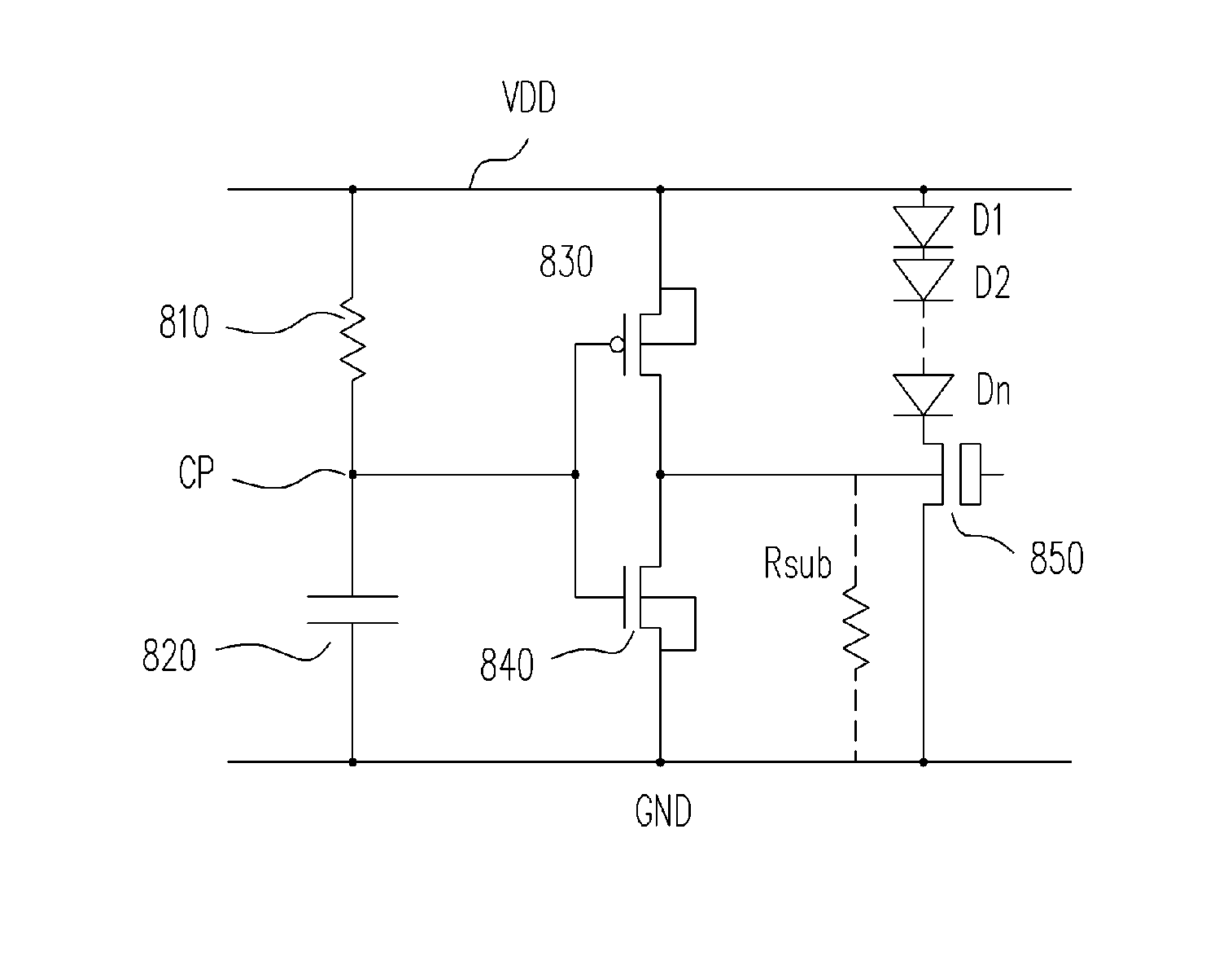
[0031]FIG. 8 is a circuit diagram of the ESD protection apparatus for high-voltage products according to the embodiments of the present invention. Referring to FIG. 8, the ESD protection apparatus includes a resistor 810, a capacitor 820, a first transistor 830, a second transistor 840, diodes D1-Dn, and a main transistor 850, wherein n is an integer greater than 0. In the embodiment, the transistors 830 and 840 are a PMOS transistor and an NMOS transistor respectively, and the main transistor 850 is an N-type field-oxide device. In general, the substrate of the main transistor 850 has a substrate-internal resistor (indicated as a resistor Rsub in FIG. 8), wherein the substrate of the main transistor 850 is coupled to the second power rail GND (as the ground line here) via the substrate-internal resistor Rsub.
[0032] The capacitor 820 and the resistor 810 are connected with each other in series between the first power rail VDD (as the system voltage line) and the second power rail G...
PUM
 Abstract
Description
Claims
Application Information
 - R&D
- Intellectual Property
- Life Sciences
- Materials
- Tech Scout
- Unparalleled Data Quality
- Higher Quality Content
- 60% Fewer Hallucinations
Browse by: Latest US Patents, China's latest patents, Technical Efficacy Thesaurus, Application Domain, Technology Topic, Popular Technical Reports.
© 2025 PatSnap. All rights reserved.Legal|Privacy policy|Modern Slavery Act Transparency Statement|Sitemap|About US| Contact US: help@patsnap.com


