Multilayer reflective film coated substrate, manufacturing method thereof, reflective mask blank, and reflective mask
a reflective film and substrate technology, applied in the direction of photomechanical treatment originals, lighting and heating apparatus, instruments, etc., can solve the problems of inability to correct both concave and convex defects solely by film forming methods, and difficulty in obtaining a highly smooth and defectless surface that can satisfy the foregoing surface roughness requirement, etc., to achieve efficient manufacturing, reduce defects, and high surface smoothness
- Summary
- Abstract
- Description
- Claims
- Application Information
AI Technical Summary
Benefits of technology
Problems solved by technology
Method used
Image
Examples
example 1
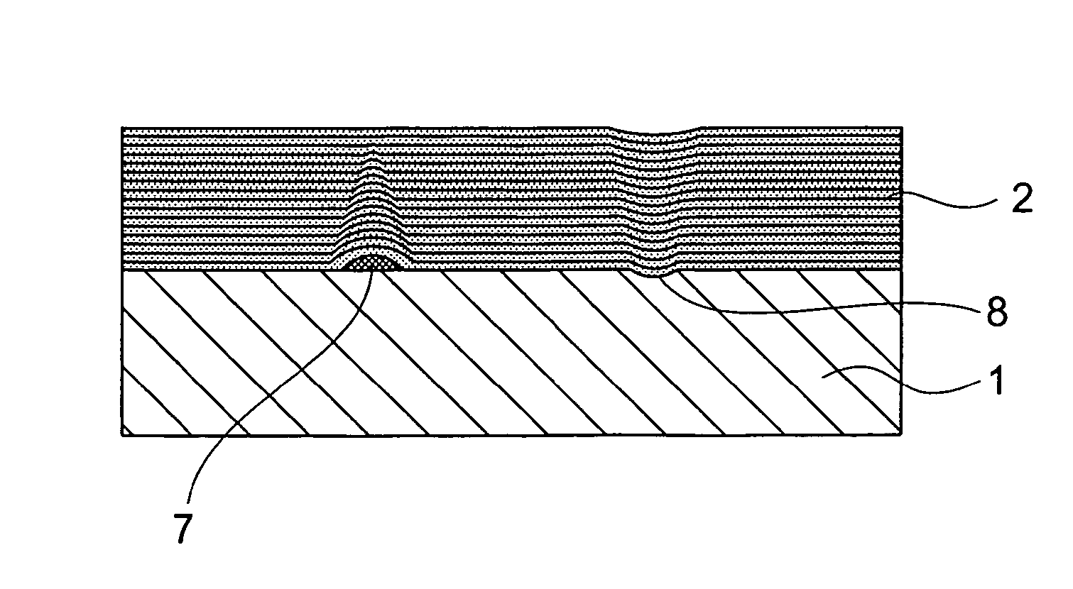
[0108] As a substrate, there was prepared a low thermal expansion SiO2—TiO2-based glass substrate having a 152 mm square shape with a thickness of 6.35 mm. This glass substrate had a smooth surface of 0.15 nmRms and a flatness of 100 nm or less by mechanical polishing and cleaning.
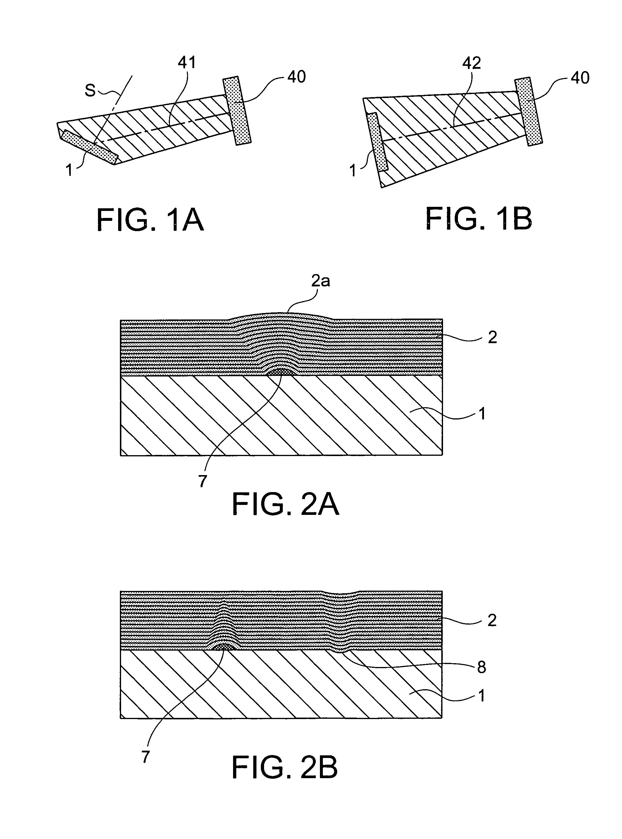
[0109] Surface defects (convex and concave defects) on the surface of the obtained glass substrate were measured by the use of a defect inspection apparatus (MAGICS M-1350 manufactured by Lasertec Corporation) and it was found that several hundreds of convex and concave defects were present over the entire substrate.
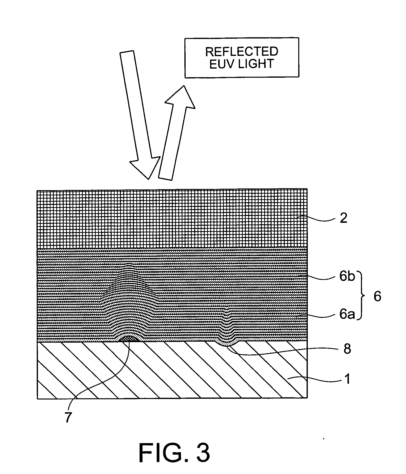
[0110] Then, a multilayer under film comprised of Mo / Si alternately-layered films was formed on the substrate. The film formation was carried out by the use of an ion beam sputtering apparatus. At first, the angle of the substrate in the apparatus was adjusted so that sputtered particles from a target were incident on the substrate from a direction inclined by 60° with respect to the perpendi...
example 2
[0118] A multilayer reflective film coated substrate was produced in the same manner as in Example 1 except that a Si film and a RuNb film were formed to thicknesses of 4.0 nm and 2.5 nm, respectively, as a capping layer on the multilayer reflective film.
[0119] The reflectance of the multilayer reflective film of this multilayer reflective film coated substrate was measured in the same manner as in Example 1 and it was 64.4%.
[0120] Further, surface defects (convex and concave defects) of the multilayer reflective film were measured by the foregoing defect inspection apparatus and several tens of surface defects were found.
example 3
[0121] A multilayer under film comprised of Mo / Si alternately-layered films was formed on the same substrate as that in Example 1. The film formation was carried out by the use of the ion beam sputtering apparatus. At first, the angle of the substrate in the apparatus was adjusted so that sputtered particles from the target were incident on the substrate from a direction inclined by 60° with respect to the perpendicular direction. Then, at first, a Si film was formed to a thickness of 2.5 nm by the use of the Si target, then a Mo film was formed to a thickness of 1.5 nm by the use of the Mo target and, given that this formed one cycle, Si and Mo films were layered by 10 cycles. Thereafter, the angle of the substrate in the apparatus was adjusted so that sputtered particles from the target were incident on the substrate from the perpendicular direction. Then, a Si film was formed to a thickness of 1.5 nm by the use of the Si target, then a Mo film was formed to a thickness of 2.5 nm ...
PUM
| Property | Measurement | Unit |
|---|---|---|
| wavelength | aaaaa | aaaaa |
| Rms) roughness | aaaaa | aaaaa |
| wavelength | aaaaa | aaaaa |
Abstract
Description
Claims
Application Information
 - R&D
- Intellectual Property
- Life Sciences
- Materials
- Tech Scout
- Unparalleled Data Quality
- Higher Quality Content
- 60% Fewer Hallucinations
Browse by: Latest US Patents, China's latest patents, Technical Efficacy Thesaurus, Application Domain, Technology Topic, Popular Technical Reports.
© 2025 PatSnap. All rights reserved.Legal|Privacy policy|Modern Slavery Act Transparency Statement|Sitemap|About US| Contact US: help@patsnap.com


