
Thermoelectric device produced by quantum confinement in nanostructures

a nano-structure, quantum confinement technology, applied in the manufacture/treatment of thermoelectric devices, thermoelectric device details, electrical apparatus, etc., can solve the problems of low efficiency, the thermoelectric technology industry standard cannot be functionally integrated into everyday heating and cooling products and systems, and the promise of practical thermoelectricity has not yet been fulfilled, etc. , to achieve the effect of increasing oxidation time, increasing oxidation time, and decreasing the thickness of the thermoelectric film

Inactive Publication Date: 2007-04-19
ZT3 TECH INC
View PDF41 Cites 8 Cited by
  • Summary
  • Abstract
  • Description
  • Claims
  • Application Information

AI Technical Summary

Benefits of technology

[0019] It is another object of the present invention to provide a method for producing practical thermoelectric devices that may be cost-effectively integrated into everyday heating and cooling products.
[0020] Additionally, it is an object of the present invention to provide a method for producing practical thermoelectric devices that provide a smaller footprint than the industry standard.
[0021] It is a further object of the present invention to provide a method for producing practical thermoelectric devices capable of being mass-produced at a lower cost than the current industry standard.
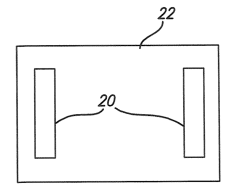
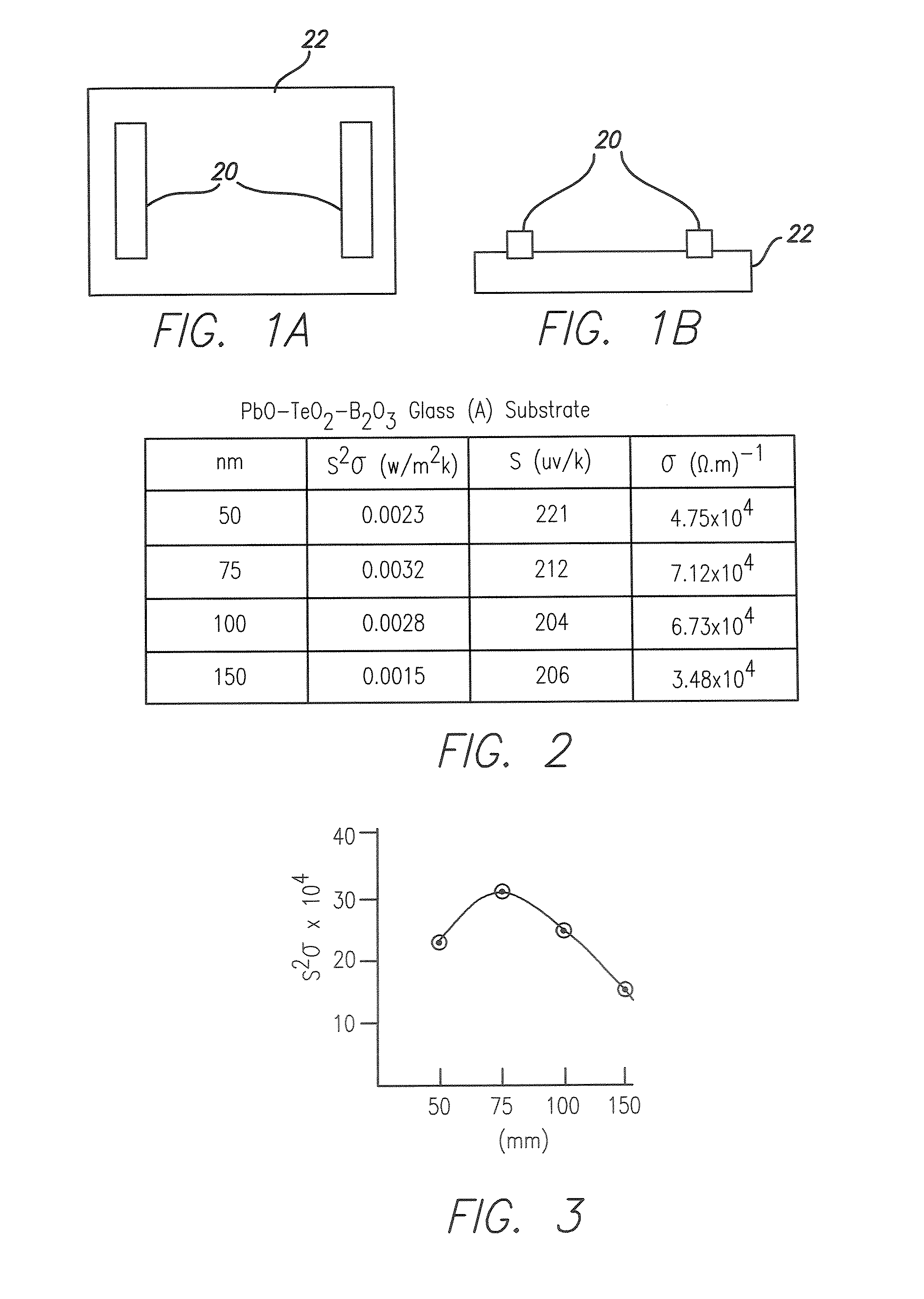
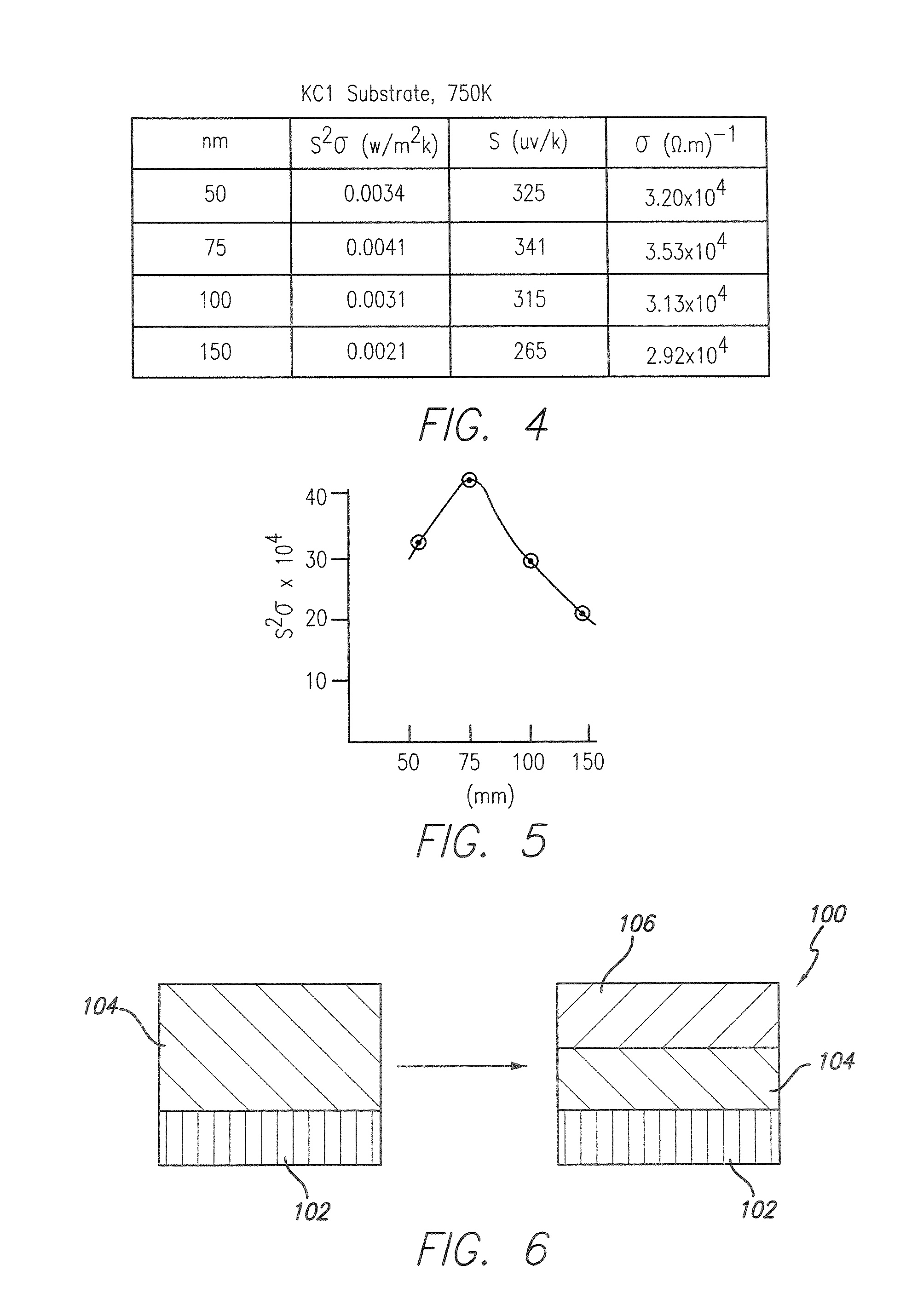
[0026] The preferred method for preparing the thermoelectric device may further comprise the step of flash heating the substrate to melt the oxide layer to convert the oxide layer from a relatively porous material into a relatively dense glassy material. The thickness of the thermoelectric film decreases with increased oxidation time, whereas the thickness of the oxide layer of PbO—TeO2 increases with increased oxidation time. The method steps may be repeated to produce a thermoelectric device having multiple thermoelectric film layers separated by insulating layers. According to the preferred embodiment, multiple thermoelectric devices of the present invention may be employed in a refrigerator, generator or Peltier device. The thermoelectric film preferably is less than 300 nm in thickness, more preferably between 50 nm and 200 nm in thickness, and most preferably between 75 nm and 100 nm in thickness. The electrodes can be formed from any material that will not melt or oxidize under the operating temperature environment to which the device is exposed. Consequently, the electrodes preferably comprise a material such as platinum, gold or silver for maximum robustness.

Problems solved by technology

However, the promise of practical thermoelectricity has not yet been fulfilled.
One problem is that, because of its low efficiency, the industry standard in thermoelectric technology cannot be functionally integrated into everyday heating and cooling products and systems.
However, the efficiency of energy conversion and / or coefficient of performance of these bulk form thermoelectric devices are considerably lower than those of conventional reciprocating or rotary heat engines and vapor- compression systems.
In view of these drawbacks and the general immaturity of the technology, bulk form thermoelectric devices have not attained immense popularity.
After four decades of research, commercially available systems are still limited to ZT values that barely approach 1.
However, these approaches are cost-prohibitive and many of the materials cannot be manufactured in significant amounts.

Method used


Image

  • Thermoelectric device produced by quantum confinement in nanostructures
  • Thermoelectric device produced by quantum confinement in nanostructures
  • Thermoelectric device produced by quantum confinement in nanostructures

Examples


Embodiment Construction

[0039] In the following paragraphs, the present invention will be described in detail by way of example with reference to the attached drawings. Throughout this description, the preferred embodiment and examples shown should be considered as exemplars, rather than as limitations on the present invention. As used herein, the “present invention” refers to any one of the embodiments of the invention described herein, and any equivalents. Furthermore, reference to various feature(s) of the “present invention” throughout this document does not mean that all claimed embodiments or methods must include the referenced feature(s).

[0040] Before starting a description of the Figures, some terms will now be defined.

[0041] Bulk Material: Macroscopic-sized thermoelectric materials that are typically larger than 1 micron or 1 micrometer in all three dimensions.

[0042] Chalcogenides: Group VI elements of the periodic table.

[0043] Chemical Vapor Deposition: Deposition of thin films (usually diele...


PUM

PropertyMeasurementUnit
thicknessaaaaaaaaaa
thicknessaaaaaaaaaa
thicknessaaaaaaaaaa

Abstract

The present invention provides a thermoelectric device comprising a film of thermoelectric material deposited on a substrate, and one or more electrodes located within the thermoelectric film, wherein the thermoelectric film is partially oxidized to form an oxide layer, which is melted to form an electrical insulating and protective barrier on a top surface of the film.

Description

FIELD OF THE INVENTION [0001] The present invention is directed to thermoelectric devices and more particularly to thermoelectric devices produced by utilizing the concepts of quantum confinement in thin films. BACKGROUND OF THE INVENTION [0002] Thermoelectric materials generate electricity when subjected to a thermal gradient and produce a thermal gradient when electric current is passed through them. Scientists have been trying to harness practical thermoelectricity for decades because practical thermoelectricity could, inter alia: (1) replace fluorocarbons used in existing cooling systems such as refrigerators and air conditioners; and (2) reduce harmful emissions during thermal power generation by converting some or most of the waste heat into electricity. However, the promise of practical thermoelectricity has not yet been fulfilled. One problem is that, because of its low efficiency, the industry standard in thermoelectric technology cannot be functionally integrated into ever...

Claims


Application Information

Patent Timeline
Patent Type & Authority Applications(United States)
IPC IPC(8): H01L35/02H10N10/80
CPCH01L35/34H10N10/01
Inventor DUTTA, BIPRODAS
Owner ZT3 TECH INC
Learn More