Method for simultaneous fabrication of a nanocrystal and non-nanocrystal device

a nanocrystal and non-nanocrystal technology, applied in the direction of semiconductor devices, electrical equipment, nanotechnology, etc., can solve the problems of affecting the performance of the fabricated device, the nanocrystal device may be exceedingly small,

Active Publication Date: 2007-04-12
ATMEL CORP
View PDF9 Cites 2 Cited by
  • Summary
  • Abstract
  • Description
  • Claims
  • Application Information

AI Technical Summary

Problems solved by technology

Nanocrystal devices may be exceedingly small since the charge storage structures have nanometer size.
Fabrication of nanocrystal devices usually requires that the thermal temperature of processing or annealing steps be as low as possible since high temperatures may cause increased dopant diffusion that adversely affects the performance of the fabricated device.

Method used


Image

  • Method for simultaneous fabrication of a nanocrystal and non-nanocrystal device
  • Method for simultaneous fabrication of a nanocrystal and non-nanocrystal device
  • Method for simultaneous fabrication of a nanocrystal and non-nanocrystal device

Examples


Embodiment Construction

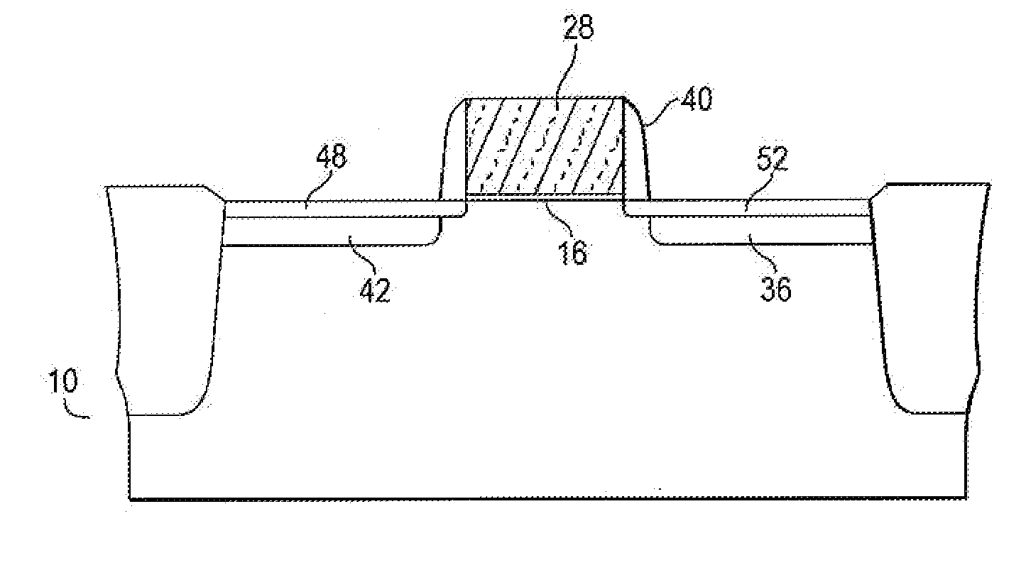
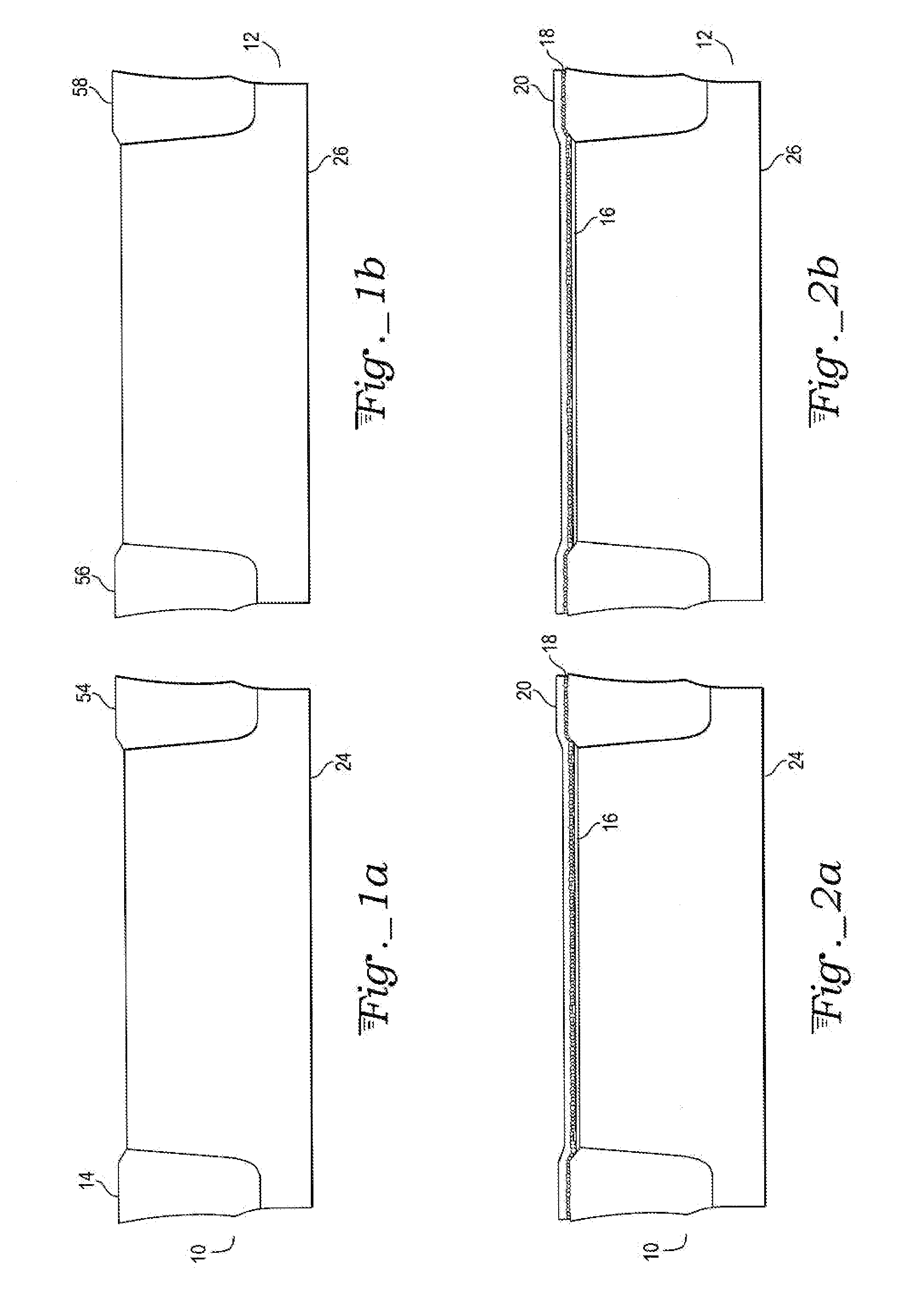
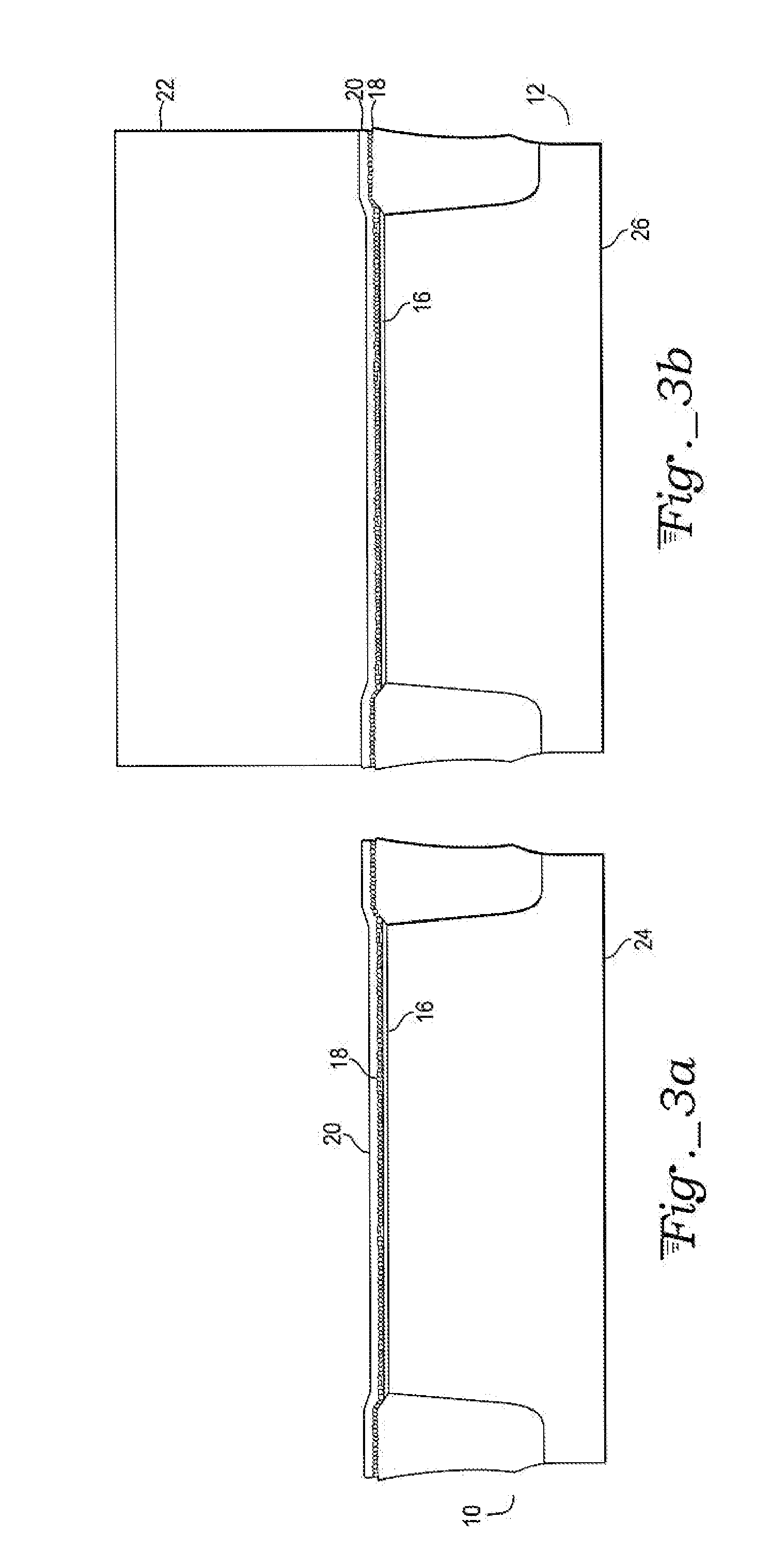
[0010] A process for simultaneously fabricating a semiconductor device, such as a memory cell, containing a nanocrystal layer as well as a peripheral semiconductor device (in one embodiment, forming CMOS transistor) that does not contain a nanocrystal layer is described below. With reference to FIGS. 1a-22a, exemplary process steps provide detail for fabrication of a peripheral device that does not contain nanocrystals while FIGS. 1b-22b provide detail for an exemplary fabrication of a memory cell containing nanocrystals.

[0011] In FIGS. 1a and 1b, a semiconductor substrate, for example p-type silicon, is provided. Assuming two semiconductor devices, a peripheral semiconductor device without nanocrystals (FIG. 1a) and a memory cell with nanocrystals (FIG. 1b) are, to be fabricated simultaneously on the substrate, both a portion 10 of the substrate 24 corresponding to the to-be fabricated peripheral device and a portion 12 of the substrates 26 corresponding to the memory cell with na...


PUM


Abstract

A method of simultaneously fabricating at least two semiconductor devices, at least bone of which is a nanocrystal memory and at least one of which is a non-nanocrystal semiconductor device. A nanocrystal layer is formed over an oxide layer of the at least two semiconductor devices being fabricated. The nanocrystal layer is removed from at least one portion of the substrate corresponding to the at least one non-nanocrystal device being fabricated. A polycrystalline gate is formed for each of the semiconductor devices being fabricated. Doping is provided to provide the source and drain regions for each of the semiconductor devices being fabricated. The substrate is thermally treated after the doping. The thermal budget of the fabrication process is not limited by this thermal treatment.

Description

CROSS-REFERENCE TO RELATED APPLICATION [0001] This is a divisional application of pending U.S. patent application Ser. No. 10 / 366,976 filed Oct. 13, 2004.FIELD OF THE INVENTION [0002] This invention relates to semiconductor device fabrication, in particular, simultaneous fabrication of nanocrystal and non-nanocrystal devices. BACKGROUND OF THE INVENTION [0003] Nanocrystals are known to effectively store small amounts of electric charge in microscopic metal or semiconductor particles involving only a few atoms. Nanocrystal devices may be exceedingly small since the charge storage structures have nanometer size. [0004] Fabrication of nanocrystal devices usually requires that the thermal temperature of processing or annealing steps be as low as possible since high temperatures may cause increased dopant diffusion that adversely affects the performance of the fabricated device. Therefore, it would be advantageous to provide a fabrication flow for fabrication of nanocrystal devices and n...

Claims


Application Information

Patent Timeline
Patent Type & Authority Applications(United States)
IPC IPC(8): H01L29/00H01L21/8238
CPCB82Y10/00H01L27/105H01L27/11526H01L27/11543H01L29/42332H01L29/7881Y10S977/701H10B41/40H10B41/48
Inventor LOJEK, BOHUMIL
Owner ATMEL CORP
Why Eureka
Try Eureka