
Manufacturing method of a semiconductor device

a manufacturing method and semiconductor technology, applied in the direction of semiconductor devices, electrical devices, transistors, etc., can solve the problems of short-channel effect of transistors, critical drawbacks of mass production of system lsis having various, and extremely short heat treatment time in such short-time heat treatment technologies, so as to reduce short-channel effect and short-channel effect, reduce short-channel effect, and prevent pattern dependency

Active Publication Date: 2007-03-08
GK BRIDGE 1
View PDF24 Cites 6 Cited by
  • Summary
  • Abstract
  • Description
  • Claims
  • Application Information

AI Technical Summary

Benefits of technology

[0030] Since the second impurity layer is formed, the effect of the invention, that is, a reduced leakage current, can be realized when a semiconductor device having, e.g., a halo region as a second impurity layer is manufactured.
[0031] In the manufacturing method of a semiconductor device according to the first, second or third aspect of the invention, the third depth is preferably in a range of 5 nm to 15 nm.
[0032] When the first impurity layer is formed at the third depth of the above range, a junction leakage current and pattern dependency can be reduced. Moreover, the first impurity layer can be used as, e.g., a drain extension having a shallow pn junction, which is advantageous for reduction in a short-channel effect.
[0033] In the manufacturing method of a semiconductor device according to the second or third aspect of the invention, the prescribed temperature of the heat treatment is preferably in a range of 475° C. to 600° C., and the activation of the first impurity layer or the activation of the first impurity layer and the second impurity layer is preferably conducted in a temperature range of 500° C. to 700° C.
[0034] By conducting the heat treatment in this temperature range for a relatively long time, that is, for several minutes, generation of pattern dependency can be prevented during restoration of the crystal structure of the amorphous layer. Moreover, by using a low temperature SPE technology in the activation of the impurity layer(s), the impurity layer(s) can be activated while suppressing generation of pattern dependency and impurity diffusion.
[0035] A pattern of a gate electrode that is formed on the semiconductor region may be non-uniformly distributed on the semiconductor region.

Problems solved by technology

With recent improvement in integration, performance, and operation speed of semiconductor integrated circuit devices, a short-channel effect of transistors has become an increasingly serious problem.
However, the heat treatment time is extremely short in such short-time heat treatment technologies.
Such variation in transistor characteristics can be a critical drawback for mass production of system LSIs having various patterns.

Method used


Image

  • Manufacturing method of a semiconductor device
  • Manufacturing method of a semiconductor device
  • Manufacturing method of a semiconductor device

Examples


first embodiment

[0072] Hereinafter, a method for manufacturing a semiconductor device according to a first embodiment of the invention will be described with reference to the accompanying drawings.

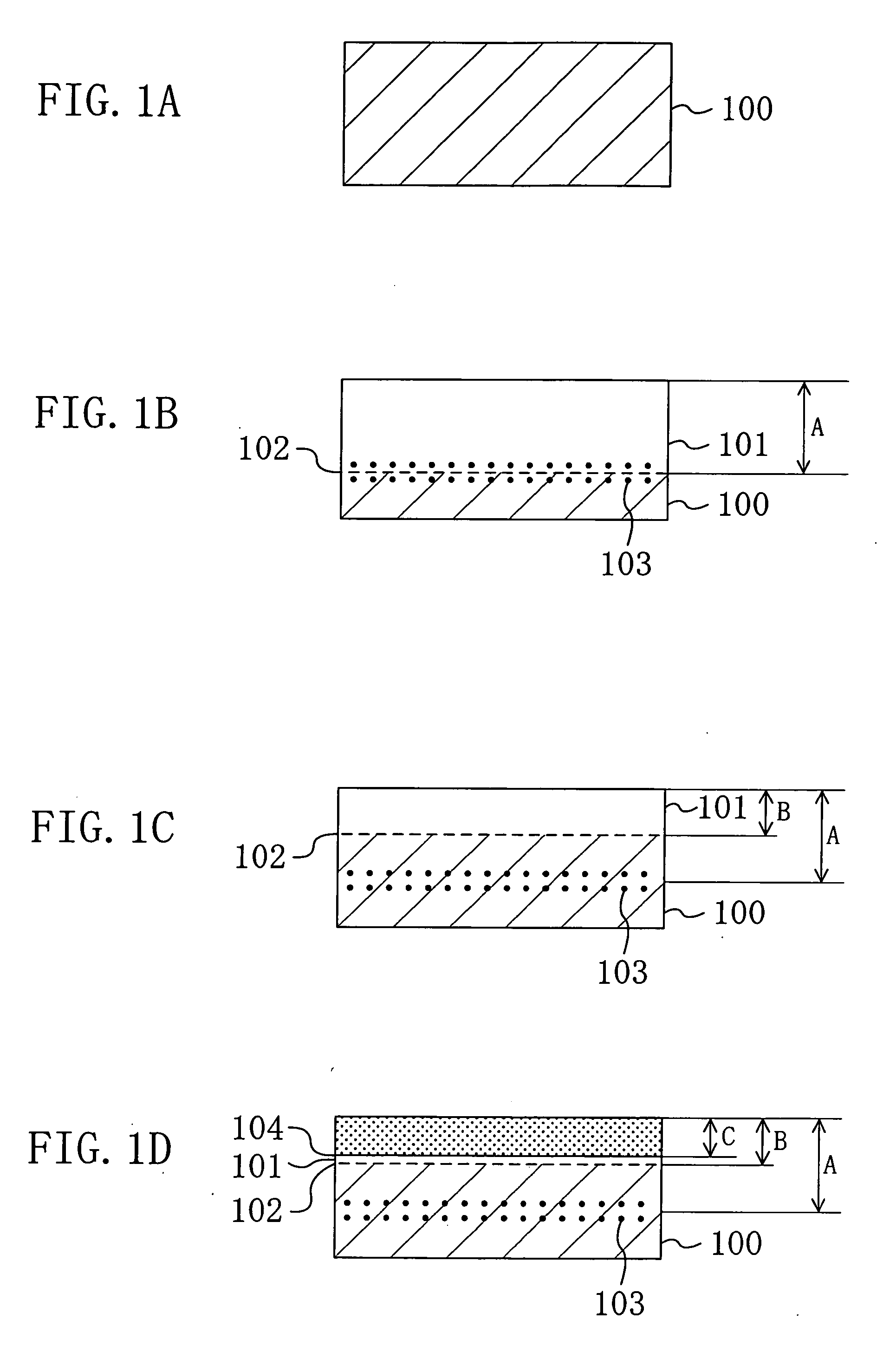
[0073] FIGS. 1(a) through 1(d) are schematic cross-sectional views showing the steps of the method for manufacturing a semiconductor device according to the first embodiment.

[0074] As shown in FIG 1(a), an n-type silicon substrate 100 is first prepared as an example of a semiconductor region.

[0075] As shown in FIG. 1(b), ions such as germanium or silicon are implanted into the silicon substrate 100 in order to form an amorphous layer 101 in the region from the surface of the silicon substrate 100 to a first depth A. At this time, defects 103 are generated near the interface between the silicon substrate 100 and a crystal region of the amorphous layer 101 (hereinafter, this interface is referred to as an amorphous-crystal interface 102), that is, near the first depth A. The first depth A for the amorpho...

second embodiment

[0085] Hereinafter, a method for manufacturing a semiconductor device according to a second embodiment of the invention will be described with reference to the accompanying drawings.

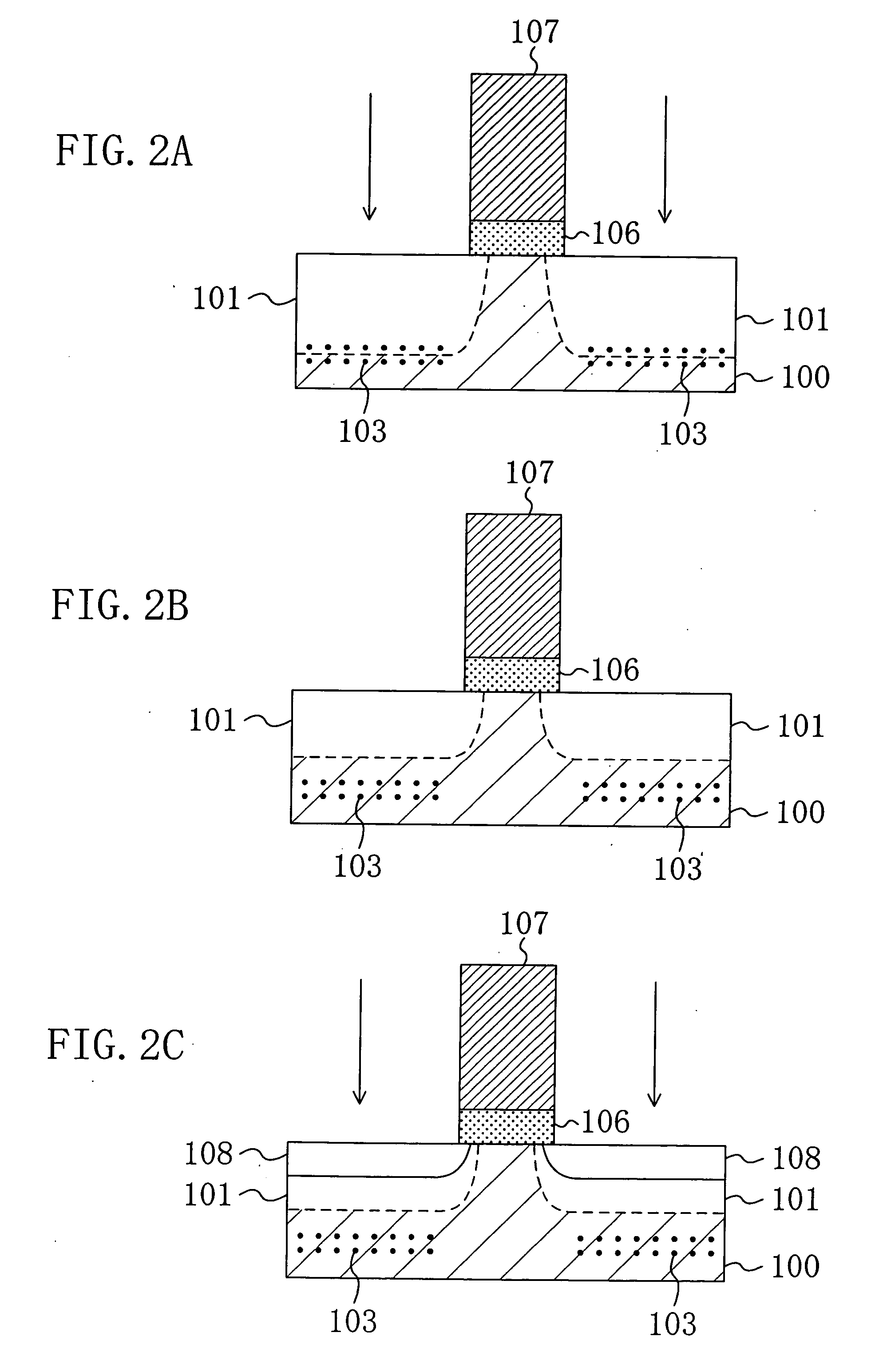
[0086] FIGS. 2(a) through 2(c) and FIGS. 3(a) through 3(c) are schematic cross-sectional views showing the steps of the method for manufacturing a semiconductor device according to the second embodiment.

[0087] As shown in FIG. 2(a), a polysilicon gate electrode 107 is formed on an n-type silicon substrate 100 as a semiconductor region with a gate insulating film 106 interposed therebetween. For example, the gate electrode 107 may be formed by using a known lithography technology and a known etching technology. For example, the gate length is 70 nm.

[0088] Ions such as germanium or silicon are implanted on both sides of the gate electrode 107 in the silicon substrate 100 in order to form an amorphous layer 101 with a thickness from the surface of the silicon substrate 100 to a first depth. The thickness...

third embodiment

[0110] Hereinafter, a method for manufacturing a semiconductor device according to a third embodiment of the invention will be described with reference to the accompanying drawings.

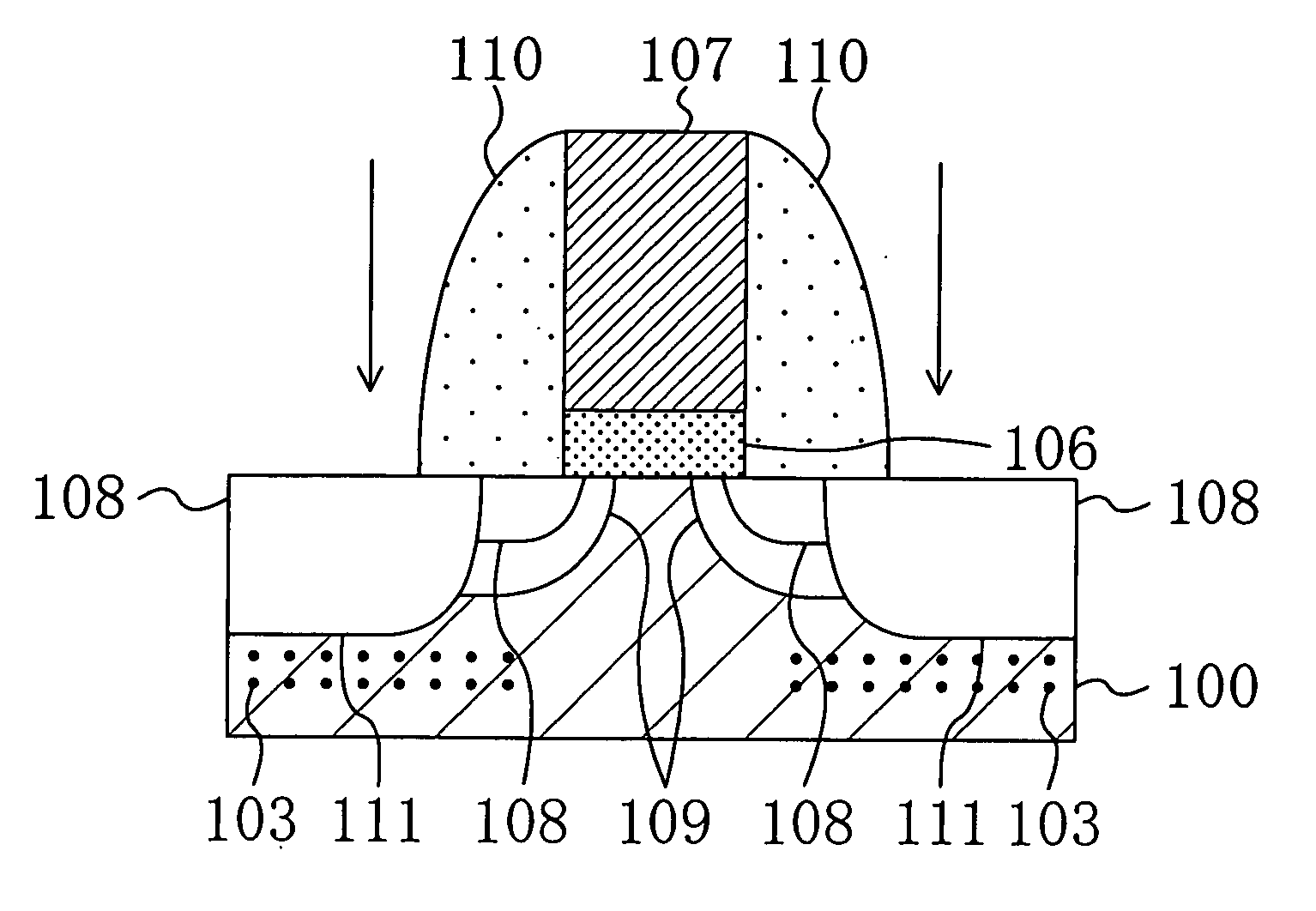
[0111] FIGS. 4(a) through 4(c) and FIGS. 5(a) through 5(c) are schematic cross-sectional views showing the steps of the method for manufacturing a semiconductor device according to the third embodiment.

[0112] First, as shown in FIG. 4(a), a polysilicon gate electrode 107 is formed on an n-type silicon substrate 100 as a semiconductor region with a gate insulating film 106 interposed therebetween. For example, the gate electrode 107 may be formed by using a known lithography technology and a known etching technology.

[0113] Thereafter, ions such as germanium or silicon are implanted on both sides of the gate electrode 107 in the silicon substrate 100 in order to form an amorphous layer 101 having a thickness from the surface of the silicon substrate 100 to a first depth. The thickness of the amorphous la...


PUM


Abstract

An amorphous layer 101 is formed in a region from a surface of a silicon substrate 100 to a first depth A. At this time, defects 103 are generated near an amorphous-crystal interface 102. By heat treatment, the crystal structure of the amorphous layer 101 is restored in a region from the first depth A to a second depth B that is shallower than the first depth A. The resultant amorphous layer 101 extends from the surface of the silicon substrate 100 to the second depth B. The defects 103 remain at the first depth A. By ion implantation, a pn junction 104 is formed at a third depth C that is shallower than the second depth B.

Description

TECHNICAL FIELD [0001] The invention generally relates to a method for manufacturing a semiconductor device. More particularly, the invention relates to a method for forming a shallow junction with a suppressed leakage current. BACKGROUND ART [0002] With recent improvement in integration, performance, and operation speed of semiconductor integrated circuit devices, a short-channel effect of transistors has become an increasingly serious problem. One of the known technologies for reducing the short-channel effect is to use a drain extension having an extremely shallow pn junction. [0003] For example, it is said that, for a transistor having a gate electrode dimension of 65 nm, a desirable pn junction depth of a drain extension is about 13 nm. Possible technologies for implementing such a pn junction depth are a flash lamp annealing technology and a laser annealing technology in both of which the thermal budget time is suppressed to several milliseconds. [0004] However, the heat treat...

Claims


Application Information

Patent Timeline
IPC IPC(8): H01L21/84H01L21/00H01L21/265H01L21/324H01L21/336H01L29/78
CPCH01L21/26506H01L21/26513H01L29/6659H01L21/324H01L21/26586
Inventor SHIBATA, SATOSHI
Owner GK BRIDGE 1
Learn More