
Optical module and optical module package

a technology of optical modules and optical modules, applied in the field of optical modules, can solve the problems of large number of problems generated by loss in lines, inability to achieve impedance matching within the desired range, and probably not matching, etc., and achieve the effect of facilitating impedance matching

Active Publication Date: 2007-03-01
ELECTRONICS & TELECOMM RES INST
View PDF57 Cites 6 Cited by
  • Summary
  • Abstract
  • Description
  • Claims
  • Application Information

AI Technical Summary

Benefits of technology

[0013] The present invention is directed to an optical module that facilitates impedance matching between an external circuit and an optical device and thus allows an RF signal inputted from the external circuit to be delivered to the optical device without any loss.

Problems solved by technology

In a conventional communication system delivering an RF signal through a line such as a copper line or a coaxial cable, a large number of problems are generated by loss in the line.
Specifically, even though the optical module is designed to match the impedance between the external circuit and the optical device, the impedance is probably not matched due to variation in device characteristics, tolerance of the packaging process, and so forth.
In addition, when the variation in device characteristics or the tolerance of the packaging process is serious, the impedance matching cannot be achieved within a desired range so that the fabricated optical module cannot be used.
In addition, since the conventional optical module uses stubs to match the impedance, an operating frequency band is difficult to be adjusted.
Also, due to a narrow bandwidth characteristic of the stub, the conventional optical module is difficult to be applied to a system requiring a wide bandwidth.
However, the bias voltage supplied through the inductor cannot be applied to other external circuit 20 due to the capacitor, and the RF signal inputted from the external circuit 20 cannot affect the bias voltage due to the inductor.

Method used


Image

  • Optical module and optical module package
  • Optical module and optical module package
  • Optical module and optical module package

Examples


Embodiment Construction

[0025] Hereinafter, an exemplary embodiment of the present invention will be described in detail. However, the present invention is not limited to the embodiments disclosed below, but can be implemented in various types. Therefore, the present embodiment is provided for complete disclosure of the present invention and to fully inform the scope of the present invention to those ordinarily skilled in the art.

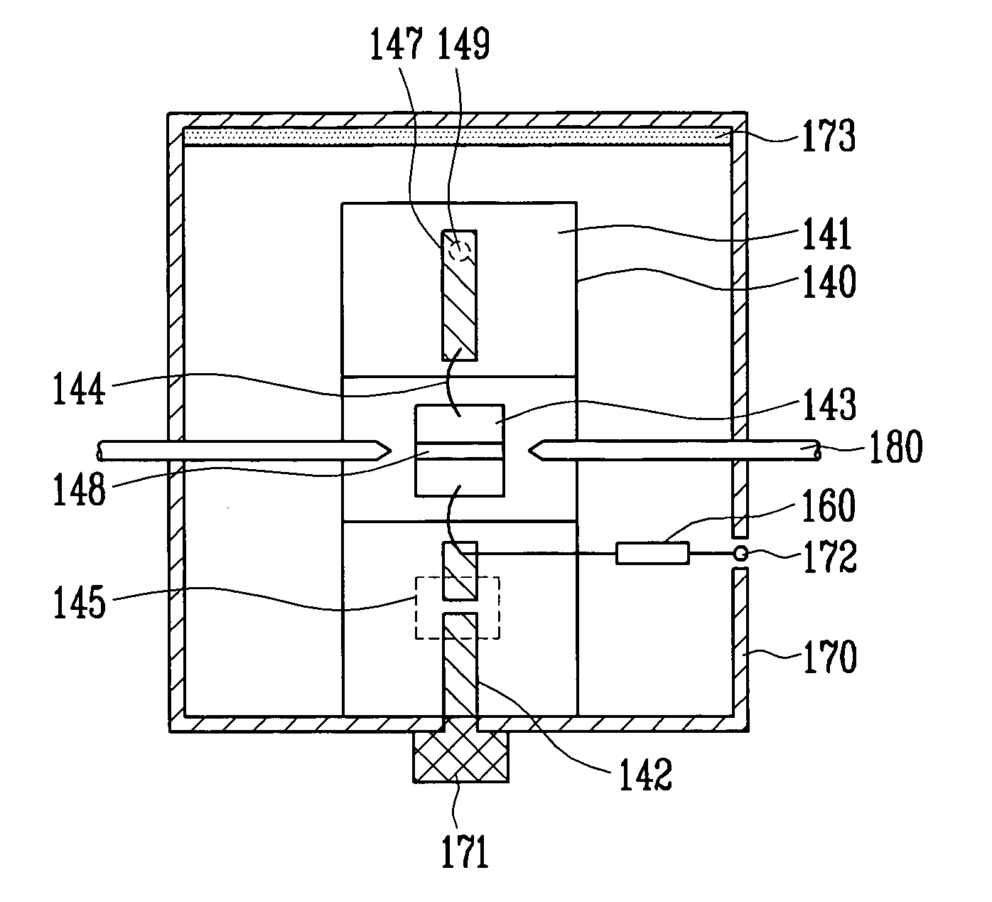
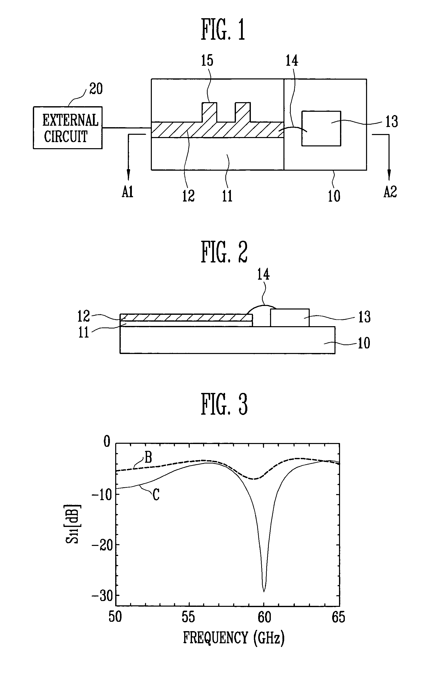
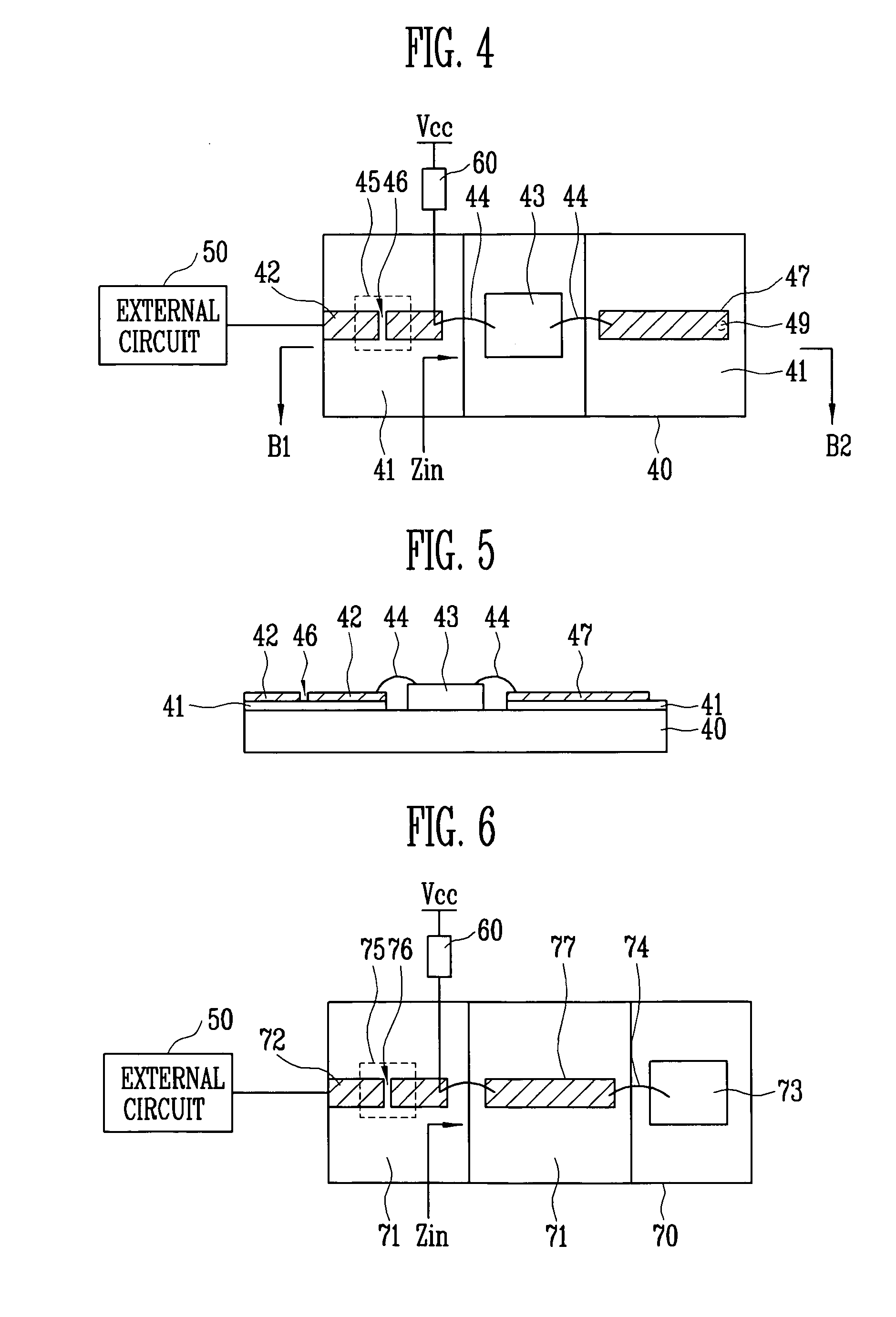
[0026] In order to fabricate an optical module required for radio over fiber (ROF) technology that delivers a radio frequency (RF) signal through an optical fiber, a packaging technique that can deliver the RF signal to a high-speed optical device such as a laser diode, an optical modulator, and an optical receiver without any loss is needed. The present invention provides an optical module for a high-speed optical device, e.g., a laser diode, an optical modulator, and an optical receiver that is used in a communication system employing the ROF technology.

[0027]FIG. 4 is a plan ...


PUM


Abstract

Provided is an optical module used in a communication system employing a radio over fiber (ROF) technology delivering a radio frequency (RF) signal through an optical fiber. The optical module includes: an optical device; a signal line for transporting a radio frequency (RF) signal input from an external circuit to the optical device; and a resistor separately disposed from the signal line and having one end connected with the optical device, wherein the input impedance seen from the signal line is matched by the resistor. A bias voltage supplied to operate the optical device is applied through an inductor connected to the signal line between the optical device and a filter. Here, the filter formed by a pattern of the signal line prevents the bias voltage from being supplied to the external circuit. In order to amplify the RF signal input from the external circuit, an amplifier may be connected between the external circuit and the filter.

Description

CROSS-REFERENCE TO RELATED APPLICATION [0001] This application claims priority to and the benefit of Korean Patent Application No. 2005-78708, filed on Aug. 26, 2005, the disclosure of which is incorporated herein by reference in its entirety. BACKGROUND [0002] 1. Field of the Invention [0003] The present invention relates to an optical module used in a wireless communication system, and more particularly, to an optical module allowing a radio frequency (RF) signal inputted from an external circuit to be delivered to an optical device without any loss in a communication system that employs radio over fiber (ROF) technology delivering an RF signal through an optical fiber. [0004] 2. Discussion of Related Art [0005] Recently, as the use of wireless communication such as Internet traffic rapidly increases, various technologies have been developed to wirelessly transmit a wideband signal to a subscriber. For wireless communication between a base station and the subscriber, information s...

Claims


Application Information

Patent Timeline
IPC IPC(8): G02B6/36G02B6/12
CPCG02B6/4201G02F1/0121H01L2224/48091H01L2924/3011H01L2924/00014H01L2924/00G02B6/4279G02B6/42
Inventor CHOI, KWANG SEONGCHUNG, YONG DUCKKANG, YOUNG SHIKJUN, DONG SUKKIM, JE HAMOON, JONG TAE
Owner ELECTRONICS & TELECOMM RES INST
Learn More