Method for manufacturing a semiconductor device
a semiconductor and manufacturing technology, applied in semiconductor devices, capacitors, electrical equipment, etc., can solve the problems of fine particles, complex structure of recent gas-feed system units containing gas piping, and inability to meet the requirements of manufacturing, so as to prevent migration on the surface of amorphous silicon film, minimize secondary growth of minute silicon nuclei thereon, easy to patterned
- Summary
- Abstract
- Description
- Claims
- Application Information
AI Technical Summary
Benefits of technology
Problems solved by technology
Method used
Image

Examples
first embodiment
(First Embodiment)
[0035] As a first embodiment, a description shall be provided of the present invention used in the polymetal gate electrode as an example.
[0036]FIGS. 1 through 6 are partial cross-sectional views of the steps of a method for manufacturing a semiconductor device according to a first embodiment of the present invention.
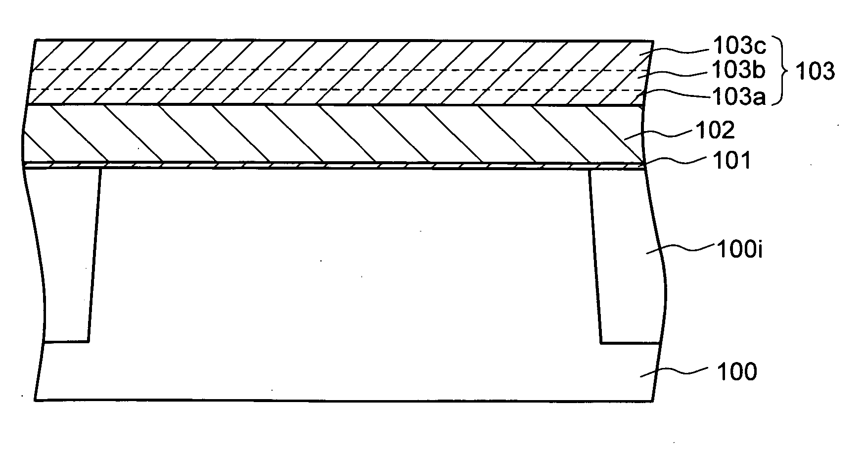
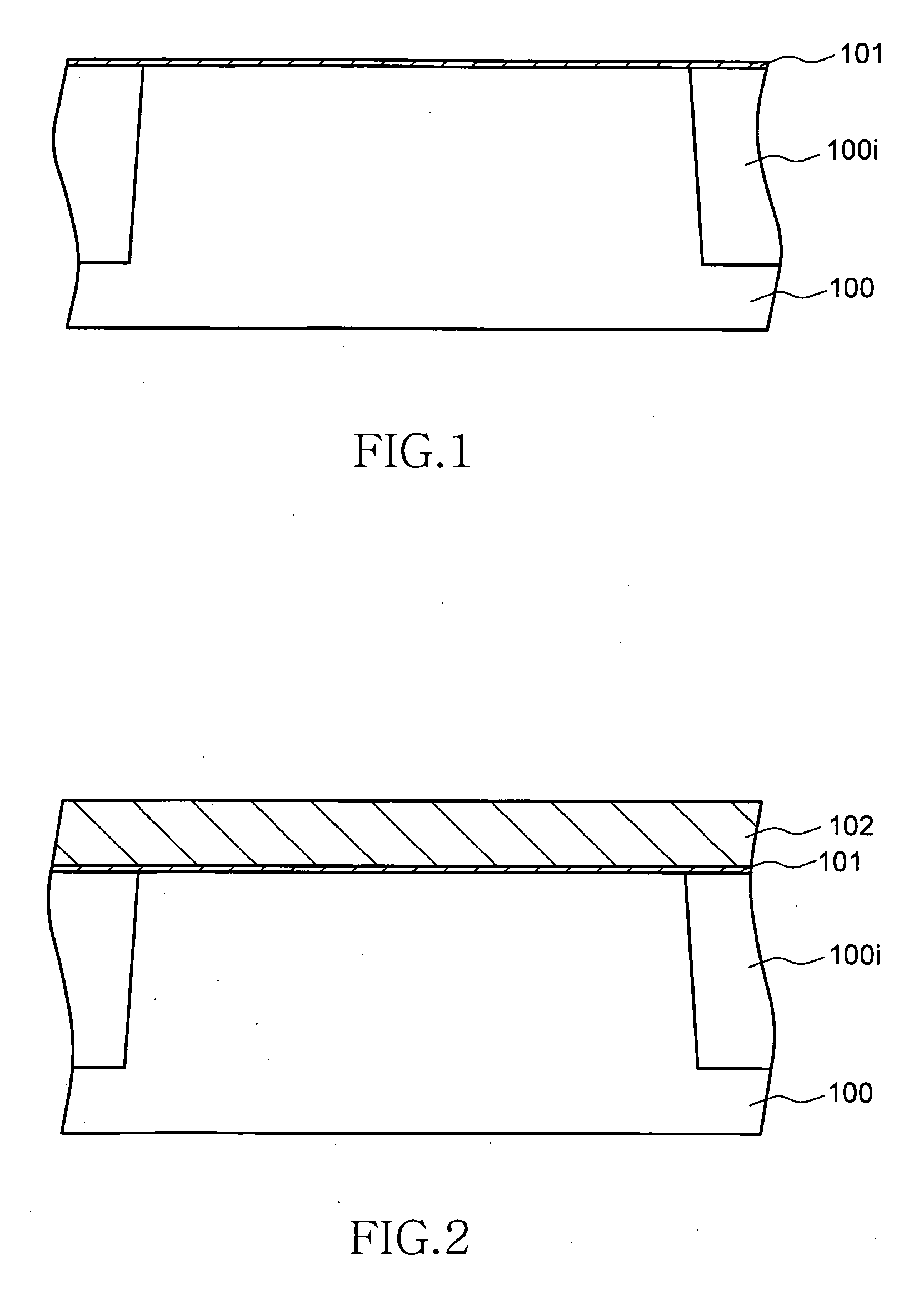
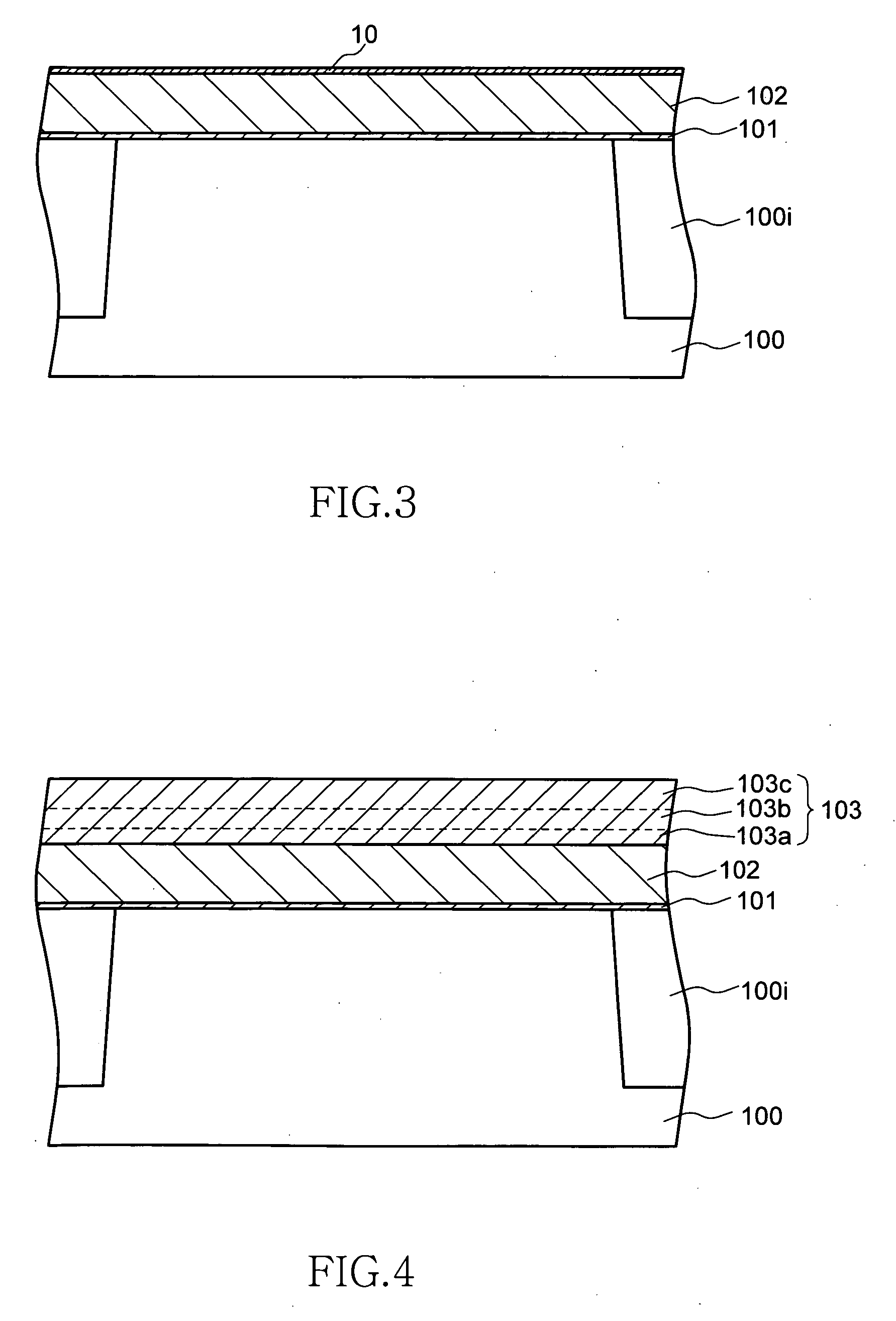
[0037] First, as shown in FIG. 1, an element-separating insulation film 100i is formed on a semiconductor substrate 100 using an existing STI (Shallow Trench Isolation) formation technique or other method, and then a gate insulation film 101 is formed on all surfaces by thermal oxidation.
[0038] Next, as shown in FIG. 2, a silicon film 102 is formed in a non-crystalline (amorphous) state on the gate insulating film 101. The silicon film 102 may either be doped with impurities or not doped with impurities.
[0039] As is shown in FIG. 3, a silicon oxide film 10 is then formed as a stopper film on the surface of the amorphous silicon film 102 to minimize...
second embodiment
(Second Embodiment)
[0049] Next, as a second embodiment, a description shall be provided of the present invention used in the bottom electrode of the cylinder-shaped capacitor as an example.
[0050]FIGS. 7 through 12 are partial cross-sectional views showing the steps of the method for manufacturing a semiconductor device according to the present embodiment, and show the steps for formation up to the bottom electrode part of the capacitor.
[0051] As shown in FIG. 7, an element-separating insulation film 200i is formed on a semiconductor substrate 200 using a known STI formation technique or the like, a gate insulating film 201 is formed on the entire surface, and a transistor gate electrode 205 and a diffusion layer 206 are subsequently formed in the element region. Next, an interlayer insulation film 207 is formed on the entire surface and a contact plug 208 connected to the diffusion layer 206 is subsequently formed. An etching stopper film 209 and a cylinder interlayer film 210 for...
PUM
| Property | Measurement | Unit |
|---|---|---|
| thickness | aaaaa | aaaaa |
| pressure | aaaaa | aaaaa |
| temperature | aaaaa | aaaaa |
Abstract
Description
Claims
Application Information
 - R&D
- Intellectual Property
- Life Sciences
- Materials
- Tech Scout
- Unparalleled Data Quality
- Higher Quality Content
- 60% Fewer Hallucinations
Browse by: Latest US Patents, China's latest patents, Technical Efficacy Thesaurus, Application Domain, Technology Topic, Popular Technical Reports.
© 2025 PatSnap. All rights reserved.Legal|Privacy policy|Modern Slavery Act Transparency Statement|Sitemap|About US| Contact US: help@patsnap.com