
Chalcogenide devices incorporating chalcogenide materials having reduced germanium or telluruim content

a technology of chalcogenide materials and chalcogenide devices, which is applied in the direction of bulk negative resistance effect devices, basic electric elements, electric devices, etc., can solve the problems of affecting the stability of the material, the material needs to be thermally stable, and the material is susceptible to variations in the structural state, so as to achieve sufficient thermal stability, improve the thermal stability of data retention, and achieve sufficient thermal stability

Inactive Publication Date: 2007-02-15
OVONYX
View PDF6 Cites 17 Cited by
  • Summary
  • Abstract
  • Description
  • Claims
  • Application Information

AI Technical Summary

Benefits of technology

"The invention provides a chalcogenide alloy composition that improves thermal stability and reduces the need for post-fabrication formation electrical stimulus in electrical chalcogenide memory applications. The alloy includes a combination of germanium (Ge) and selenium (Sb) with atomic concentrations of Ge ranging from 15% to 20% and Sb ranging from 30% to 50%. The alloy can also include tellurium (Te) with atomic concentrations ranging from 20% to 50%. The use of this alloy results in faster operation through shorter time-to-set characteristics and reduced number of electrical pulses required for device formation. The resistance of the device stabilizes in a fewer number of cycles of setting and resetting, and the thermal stability of data retention is improved. The alloy can be used in electrical devices containing a layer of chalcogenide material in electrical communication with two electrical terminals or contacts."

Problems solved by technology

A current issue in terms of the properties of chalcogenide materials is the need to improve the thermal stability of the materials.
Data in a chalcogenide material are retained as a structural state of the material, so any tendency of the structural state to transform with temperature represents a potential undesirable mechanism of erasing or losing data.
Many chalcogenide memory materials retain their structural states for long periods of time at room temperature, but become susceptible to variations in the structural state upon increasing temperature.
In practical terms, this limits the temperature environment in which chalcogenide memory devices can be utilized as well as the temperatures that can be employed in processing or manufacturing.
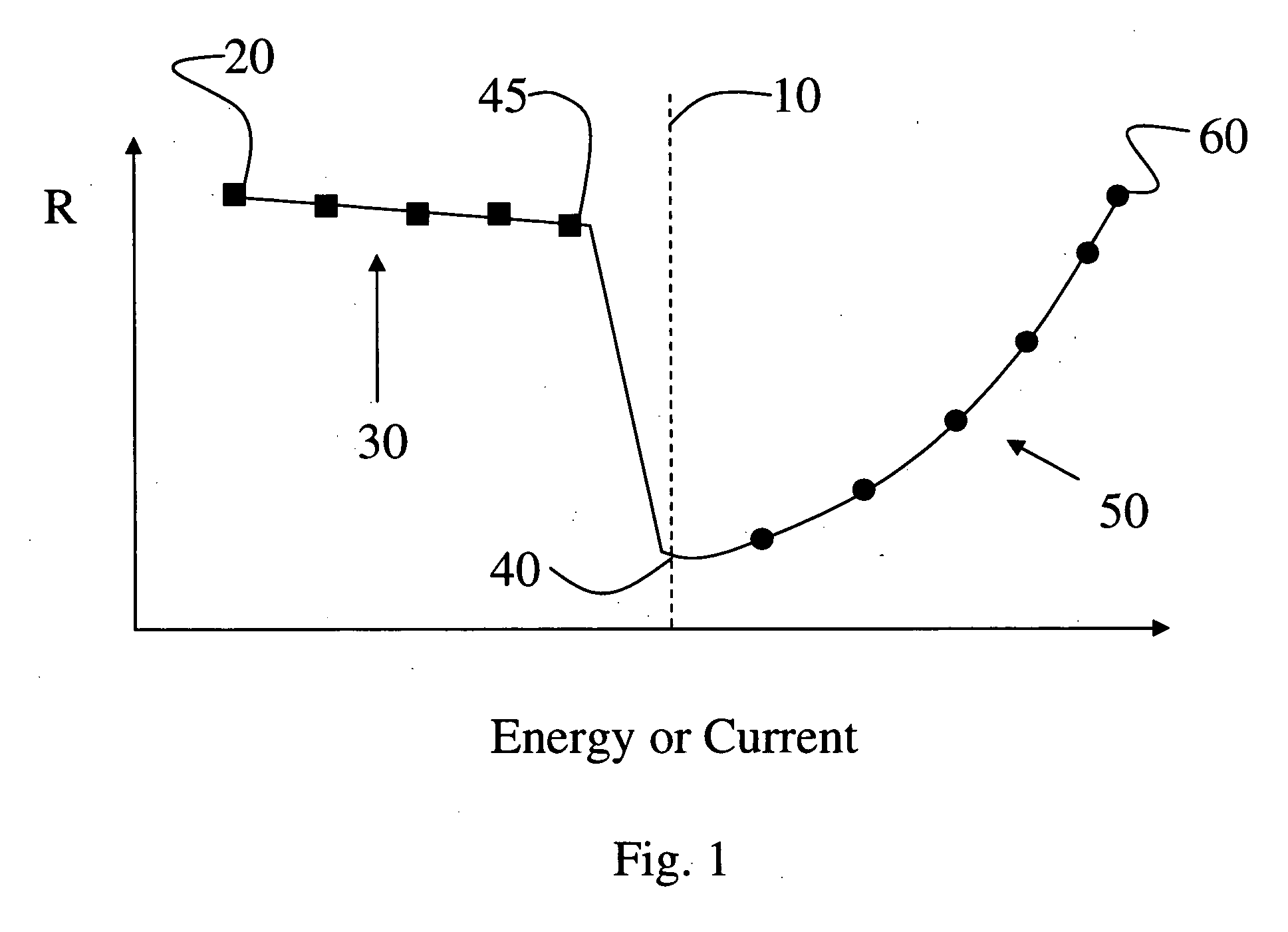
In practice, however, formation of the chalcogenide materials in current use requires many cycles of setting and resetting until the resistance of the set state stabilizes to a reproducible value.

Method used


Image

  • Chalcogenide devices incorporating chalcogenide materials having reduced germanium or telluruim content
  • Chalcogenide devices incorporating chalcogenide materials having reduced germanium or telluruim content
  • Chalcogenide devices incorporating chalcogenide materials having reduced germanium or telluruim content

Examples


example 1

[0048] In this example, the fabrication of memory devices having active chalcogenide layers in accordance with the instant invention is described. The device structure is a commonly utilized two-terminal device design having an active chalcogenide layer in a pore geometry in electrical contact with top and bottom electrodes. Two different device configurations were used and similar results were achieved for each. Both designs were deposited on an Si wafer with a thick SiO2 surface oxide layer.

[0049] In one design, a tungsten layer was deposited on the surface oxide and another SiO2 layer was deposited thereon. A 600 Å diameter opening was formed in the deposited SiO2 layer and was filled with TiN. The tungsten layer and TiN layers serves as a bottom electrode. A chalcogenide layer having a thickness of 500 Å was deposited on the TiN filled opening and surrounding SiO2 layers. A top electrode was next deposited in situ and included a 400 Å carbon layer deposited on top of the chalco...

example 2

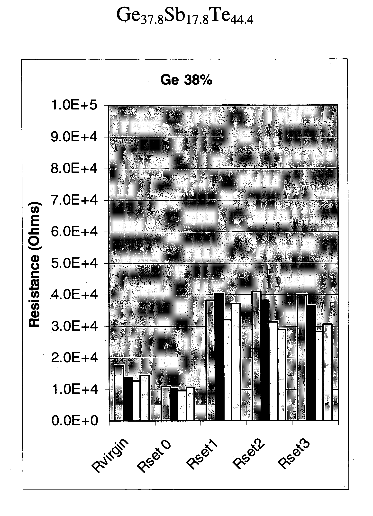
[0053] In this example, the improved formation characteristics of devices according to the instant invention are described. As described hereinabove, formation is a process that involves the post-fabrication electrical conditioning of a device to prepare it for its end application. Formation is required for the currently available chalcogenide memory devices and requires a series of electrical conditioning cycles that include setting and resetting the device until stable resistances are achieved for the set and reset states. In this example, we demonstrate the ability of devices using the instant chalcogenide materials to reduce or eliminate the need for formation. The devices used in this example correspond to those described in EXAMPLE 1 hereinabove. Devices included selected chalcogenide compositions from those presented in EXAMPLE 1 are described.

[0054] To evaluate the formation requirements of a device, we measured the resistance of the device in its as-fabricated state and su...

example 3

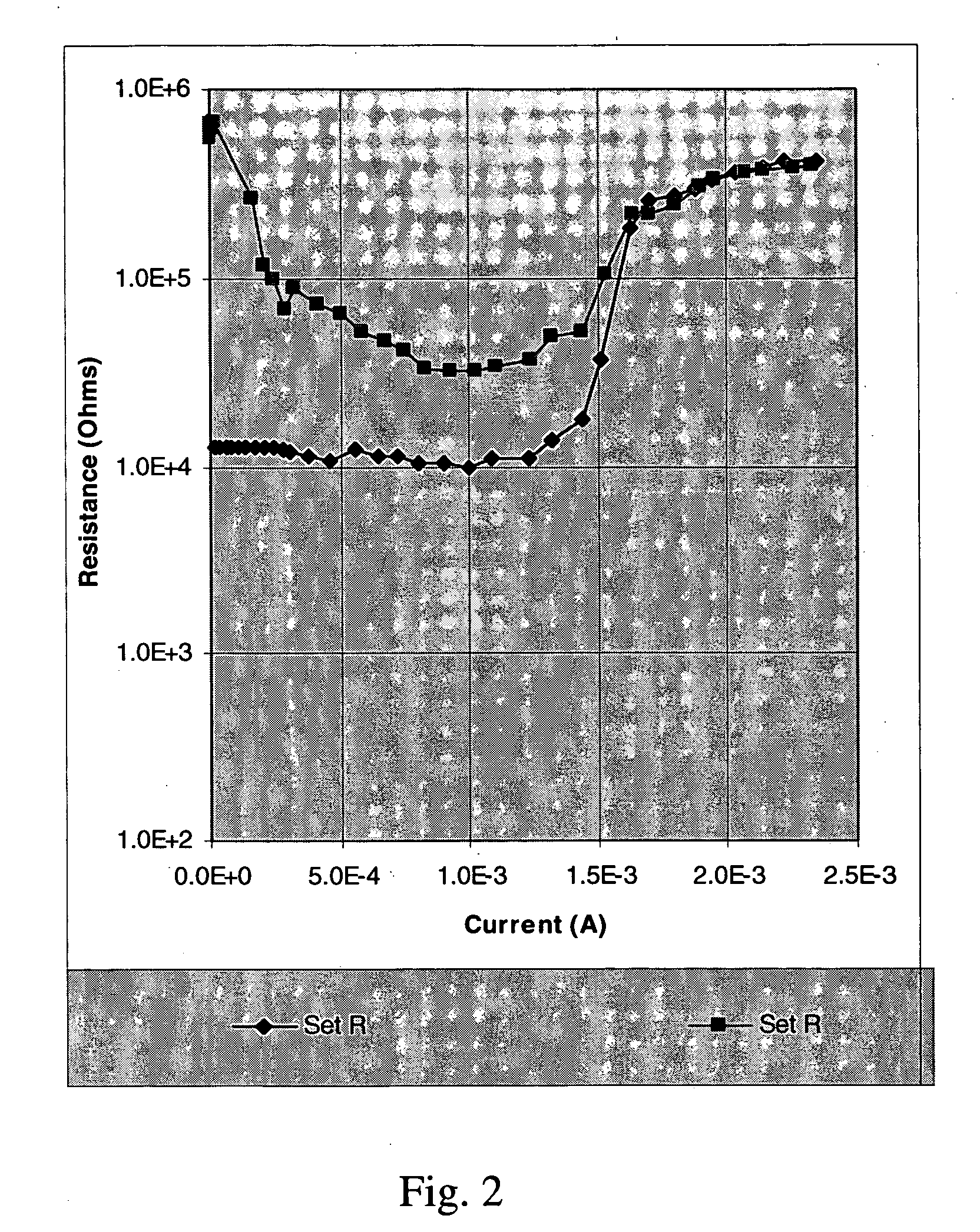
[0070] In this example, the speed advantage of the instant devices is demonstrated. During operation of a memory device, it is necessary to program the device into and out of the set and reset states in most applications. Since establishment of the reset state can generally be accomplished on shorter time scales than establishment of the set state, the programming speed of the device is controlled by the time required for setting. (Typically, the time required to set (time-to-set) is a factor of 10 or more greater than the time to reset.) Since the time-to-set is governed by the underlying crystallization process, it is desirable to develop chalcogenide materials suitable for use in memory devices that exhibit fast crystallization so that the set speed of the device can be shortened. The devices used in this example correspond to those described in EXAMPLE 1 hereinabove. Devices included selected chalcogenide compositions from those presented in EXAMPLE 1 are described.

[0071] In th...


PUM

PropertyMeasurementUnit
temperatureaaaaaaaaaa

Abstract

A chalcogenide material and chalcogenide memory device having less stringent requirements for formation, improved thermal stability and / or faster operation. The chalcogenide materials include materials comprising Ge, Sb and Te in which the Ge and / or Te content is lean relative to the commonly used Ge2Sb2Te5 chalcogenide composition. Electrical devices containing the instant chalcogenide materials show a rapid convergence of the set resistance during cycles of setting and resetting the device from its as-fabricated state, thus leading to a reduced or eliminated need to subject the device to post-fabrication electrical formation prior to end-use operation. Improved thermal stability is manifested in terms of prolonged stability of the resistance of the device at elevated temperatures, which leads to an inhibition of thermally induced setting of the reset state in the device. Significant improvements in the 10 year data retention temperature are demonstrated. Faster device operation is achieved through an increased speed of crystallization, which acts to shorten the time required to transform the chalcogenide material from its reset state to its set state in an electrical memory device.

Description

FIELD OF INVENTION [0001] This invention pertains to chalcogenide materials having applications as electrical and optical memories and switches. More particularly, this invention relates to chalcogenide materials showing high reproducibility of electrical resistance upon transformation from a primarily amorphous state to a primarily crystalline state on repeated cycles and to chalcogenide materials exhibiting high thermal stability. Most specifically, this invention is concerned with off-tieline chalcogenide alloys in the Ge—Sb—Te family having a low Ge concentration. BACKGROUND OF THE INVENTION [0002] Chalcogenide materials are an emerging class of commercial electronic materials that exhibit switching, memory, logic, and processing functionality. The basic principles of chalcogenide materials were developed by S. R. Ovshinsky in the 1960's and much effort by him and others around the world since then have led to advancements of the underlying science and an expansion of the field ...

Claims


Application Information

Patent Timeline
Patent Type & Authority Applications(United States)
IPC IPC(8): H01L47/00H10N80/00
CPCH01L45/06H01L45/1625H01L45/144H01L45/1233H10N70/231H10N70/026H10N70/826H10N70/8828
Inventor KOSTYLEV, SERGEYLOWREY, TYLERWICKER, GUYCZUBATYJ, WOLODYMYR
Owner OVONYX
Learn More