Semiconductor device

a technology of semiconductor elements and devices, applied in semiconductor devices, semiconductor/solid-state device details, electrical apparatus, etc., can solve problems such as impairment of characteristics of semiconductor elements such as mis transistors

Inactive Publication Date: 2007-01-25
SEIKO EPSON CORP
View PDF15 Cites 1 Cited by
  • Summary
  • Abstract
  • Description
  • Claims
  • Application Information

AI Technical Summary

Benefits of technology

[0003] In related-art technology, when a semiconductor element such as a MIS transistor is disposed under a pad, the characteristics of the semiconductor element such as a MIS transistor may be impaired due to stress during bonding. Therefore, the pad formation region and the semiconductor element formation region are separately provided in a semiconductor chip when viewed from the top side. However, since the semiconductor chip has been scaled down and increased in degree of integration, disposition of the semiconductor element under the pad has been demanded. JP-A-2002-319587 discloses such technology, for example.
[0037] In the semiconductor device according to this embodiment, stress tends to occur after formation of the electrode pad in a specific range positioned outward from a line extending vertically downward from the edge of at least part of the electrode pad. Therefore, cracks tend to occur in the interlayer dielectric disposed in this specific area. For example, when a semiconductor element such as a MIS transistor is formed in the semiconductor layer in this specific area, the characteristics of the MIS transistor may deteriorate. In the semiconductor device according to this embodiment, the above problem is eliminated by providing the forbidden region in this specific region. Moreover, this embodiment can provide a semiconductor device which is scaled down due to an increase in the degree of integration of elements and provided with improved reliability by disposing an element under the electrode pad at a position in which the element can be formed without causing a problem. According to this embodiment, since the connection section in which the first conductive layer and the second conductive layer are connected is not disposed in the forbidden region, cracks do not occur in the conductive layer.

Problems solved by technology

In related-art technology, when a semiconductor element such as a MIS transistor is disposed under a pad, the characteristics of the semiconductor element such as a MIS transistor may be impaired due to stress during bonding.

Method used


Image

  • Semiconductor device
  • Semiconductor device
  • Semiconductor device

Examples


first embodiment

1. First Embodiment

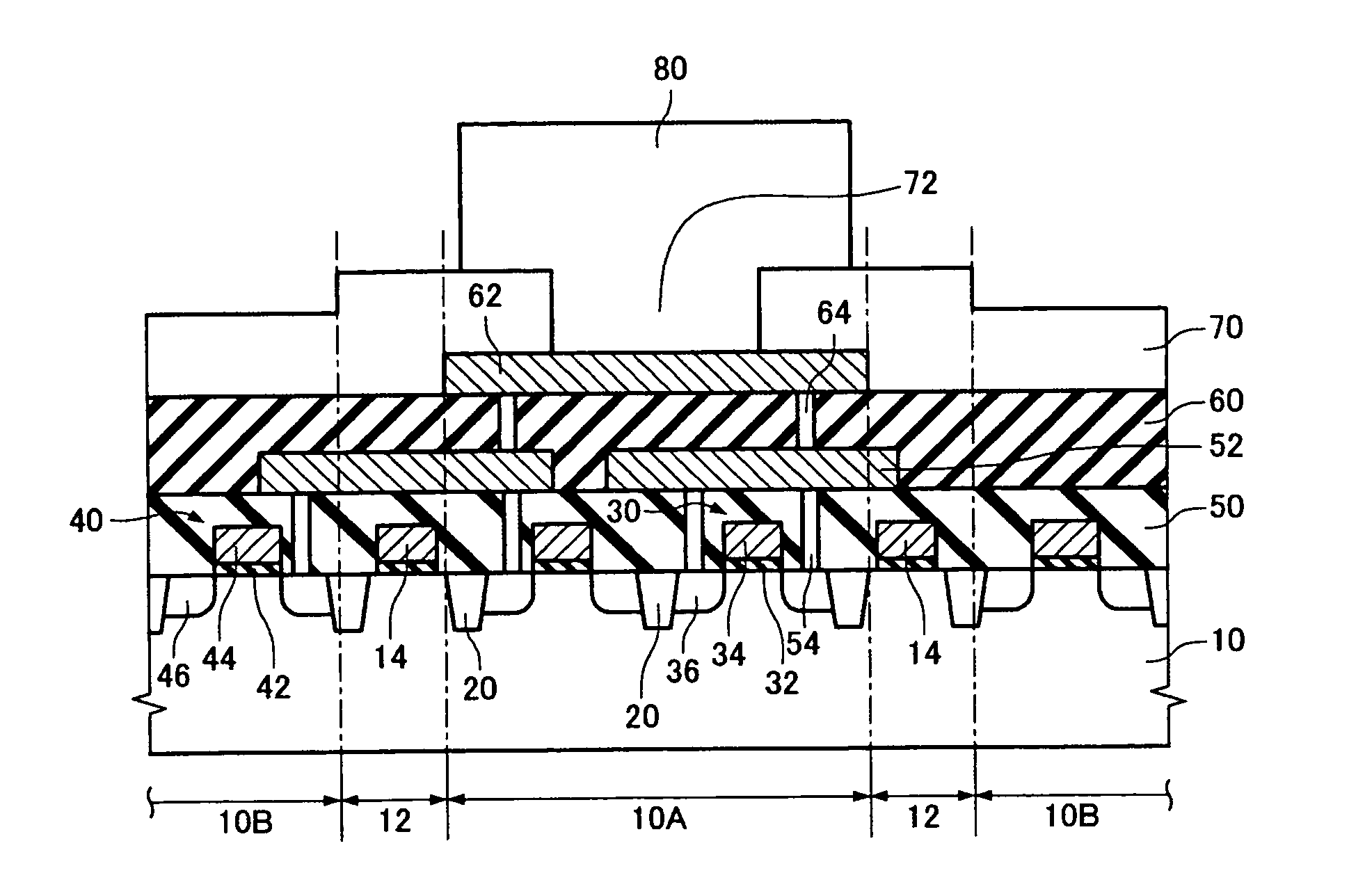
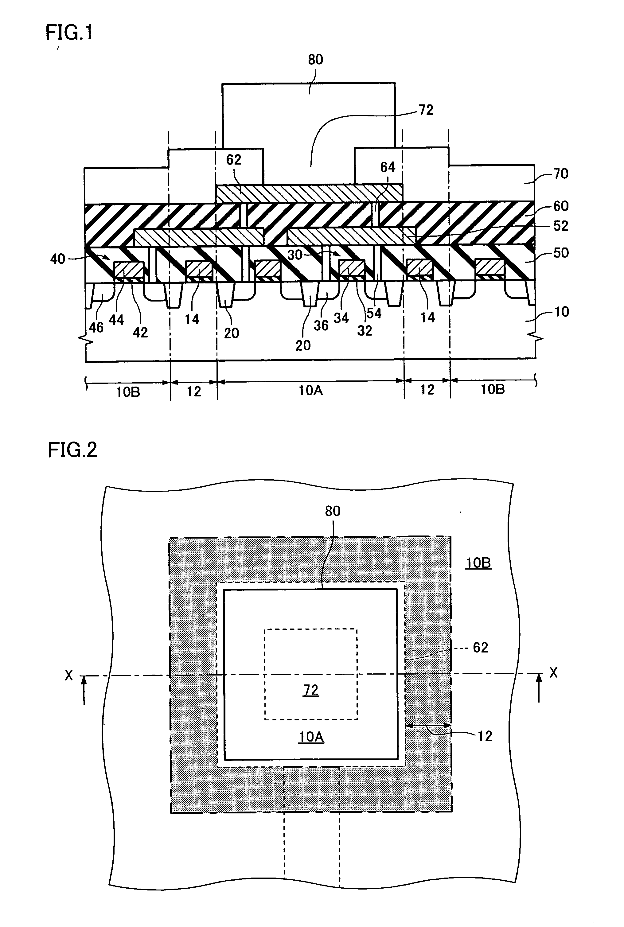
[0068]FIG. 1 is a cross-sectional view schematically showing a semiconductor device according to a first embodiment of the invention, and FIG. 2 is a plan view schematically showing the relationship between the shape of an electrode pad and a forbidden region in the semiconductor device according to the first embodiment. FIG. 1 shows the cross section along the line X-X shown in FIG. 2.

[0069] As shown in FIG. 1, the semiconductor device according to the first embodiment includes a semiconductor layer 10. As the semiconductor layer 10, a single crystal silicon substrate, a silicon on insulator (SOI) substrate in which a semiconductor layer is formed on an insulating layer, the semiconductor layer being a silicon layer, a germanium layer, or a silicon germanium layer, or the like may be used.

[0070] An isolation insulating layer 20 is formed in the semiconductor layer 10. The isolation insulating layer 20 may be formed by a shallow trench isolation (STI) method, a ...

second embodiment

2. Second Embodiment

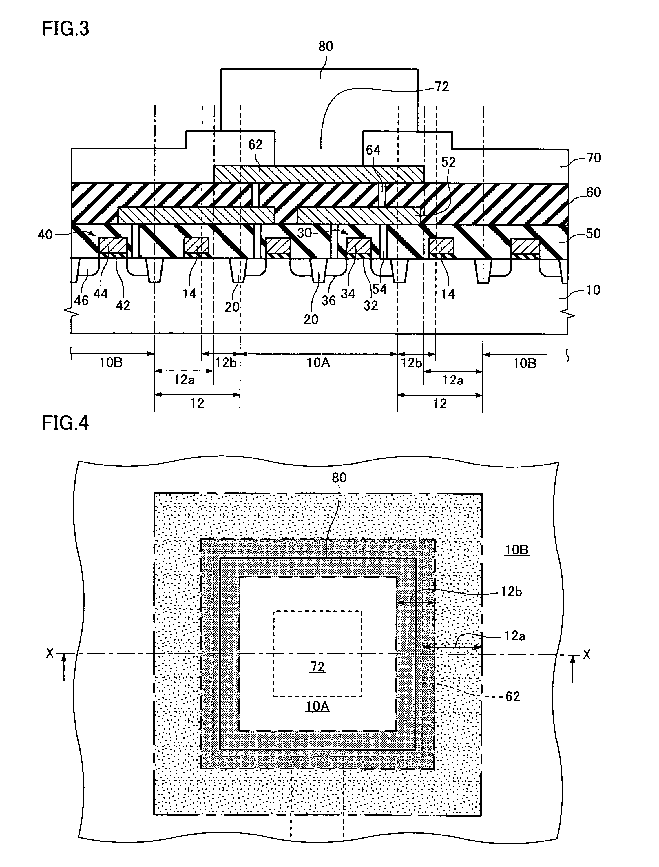
[0085] A second embodiment of the invention is described below with reference to FIGS. 3 and 4.

[0086]FIG. 3 is a cross-sectional view schematically showing a semiconductor device according to the second embodiment, and FIG. 4 is a plan view schematically showing the relationship between an electrode pad and a forbidden region in the semiconductor device according to the second embodiment. FIG. 3 shows the cross section along the line X-X shown in FIG. 4. Note that members substantially the same as the members in the first embodiment are assigned the same symbols. Detailed description of these members is omitted.

[0087] The semiconductor device according to the second embodiment differs from the semiconductor device according to the first embodiment in that the forbidden region 12 is specified taking into consideration the bump 80 in addition to the electrode pad 62 described in the first embodiment. In the second embodiment, the forbidden region 12 includes a fi...

third embodiment

3. Third Embodiment

[0095] A third embodiment of the invention is described below with reference to FIG. 5. FIG. 5 is a cross-sectional view schematically showing a semiconductor device according to the third embodiment. The semiconductor device according to the third embodiment differs from the semiconductor devices according to the first and second embodiments in that a specific semiconductor element is formed in the forbidden region 12. The following description merely illustrates the difference from the semiconductor device according to the first embodiment. Note that members substantially the same as the members of the semiconductor device according to the first embodiment are assigned the same symbols. Detailed description of these members is omitted.

[0096] As shown in FIG. 5, the semiconductor device according to the third embodiment includes the active region 10A and the forbidden region 12 provided around the active region 10A. In the semiconductor device according to the t...


PUM


Abstract

A semiconductor device, including: a semiconductor layer having an active region; a first conductive layer formed above the semiconductor layer and having a first width; a second conductive layer connected to the first conductive layer and having a second width smaller than the first width; an interlayer dielectric formed above the semiconductor layer; an electrode pad formed above the interlayer dielectric and covering the active region when viewed from a top side; and a forbidden region provided in the semiconductor layer in a specific range positioned outward from a line extending vertically downward from an edge of at least part of the electrode pad. A connection section at which the first conductive layer and the second conductive layer are connected is not provided in the forbidden region.

Description

[0001] Japanese Patent Application No. 2005-208666, filed on Jul. 19, 2005, is hereby incorporated by reference in its entirety. BACKGROUND OF THE INVENTION [0002] The present invention relates to a semiconductor device. [0003] In related-art technology, when a semiconductor element such as a MIS transistor is disposed under a pad, the characteristics of the semiconductor element such as a MIS transistor may be impaired due to stress during bonding. Therefore, the pad formation region and the semiconductor element formation region are separately provided in a semiconductor chip when viewed from the top side. However, since the semiconductor chip has been scaled down and increased in degree of integration, disposition of the semiconductor element under the pad has been demanded. JP-A-2002-319587 discloses such technology, for example. SUMMARY [0004] According to a first aspect of the invention, there is provided a semiconductor device, comprising: [0005] a semiconductor layer having ...

Claims


Application Information

Patent Timeline
IPC IPC(8): H01L23/48
CPCH01L21/823475H01L2924/01006H01L24/05H01L27/0203H01L27/088H01L2224/02166H01L2224/05093H01L2224/05095H01L2224/05644H01L2224/05647H01L2224/05655H01L2924/01004H01L2924/01005H01L2924/01013H01L2924/01014H01L2924/01015H01L2924/01022H01L2924/01028H01L2924/01029H01L2924/01032H01L2924/01033H01L2924/01074H01L2924/01078H01L2924/01079H01L2924/01082H01L2924/19043H01L23/528H01L2924/00014H01L27/092
Inventor YUZAWA, TAKESHITAGAKI, MASATOSHI
Owner SEIKO EPSON CORP
Why Eureka
Try Eureka