Method of forming openings in an organic resin material
a technology of organic resin and openings, which is applied in the direction of printing, semiconductor devices, energy conversion devices, etc., can solve the problems of reducing the performance reducing the efficiency of the end product, and quickly outweighing the cost savings of material costs
- Summary
- Abstract
- Description
- Claims
- Application Information
AI Technical Summary
Problems solved by technology
Method used
Image
Examples
Embodiment Construction
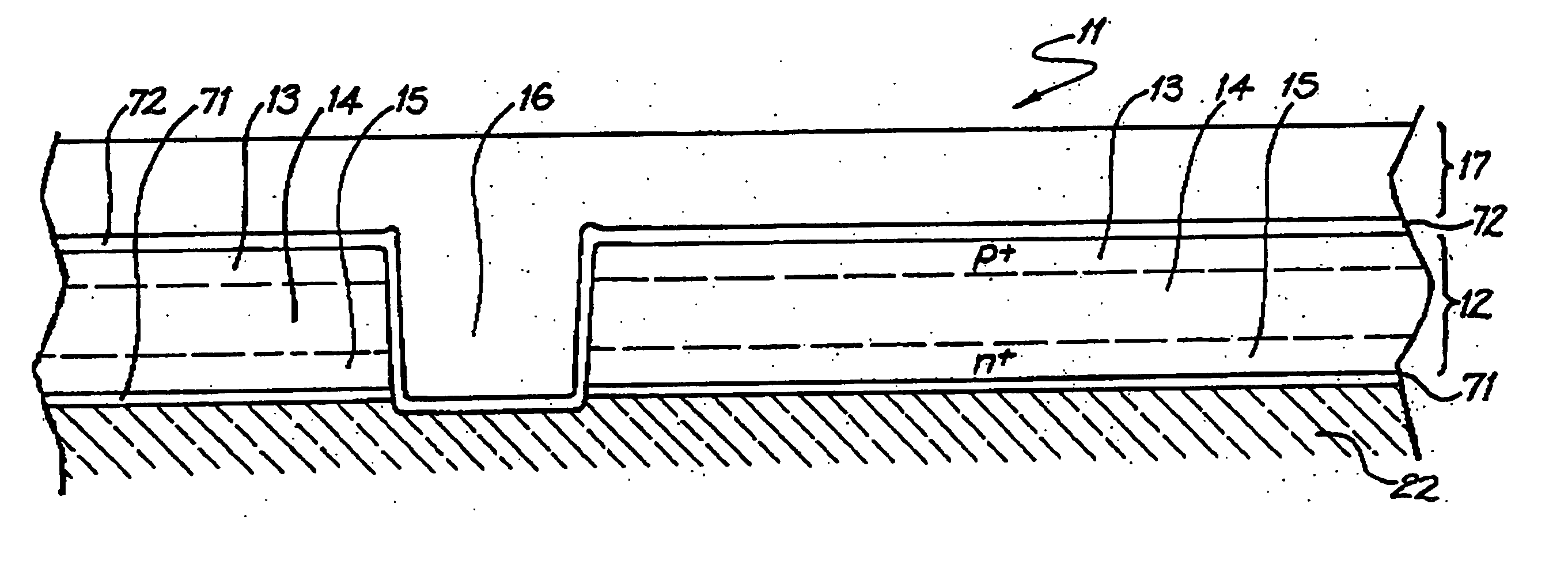
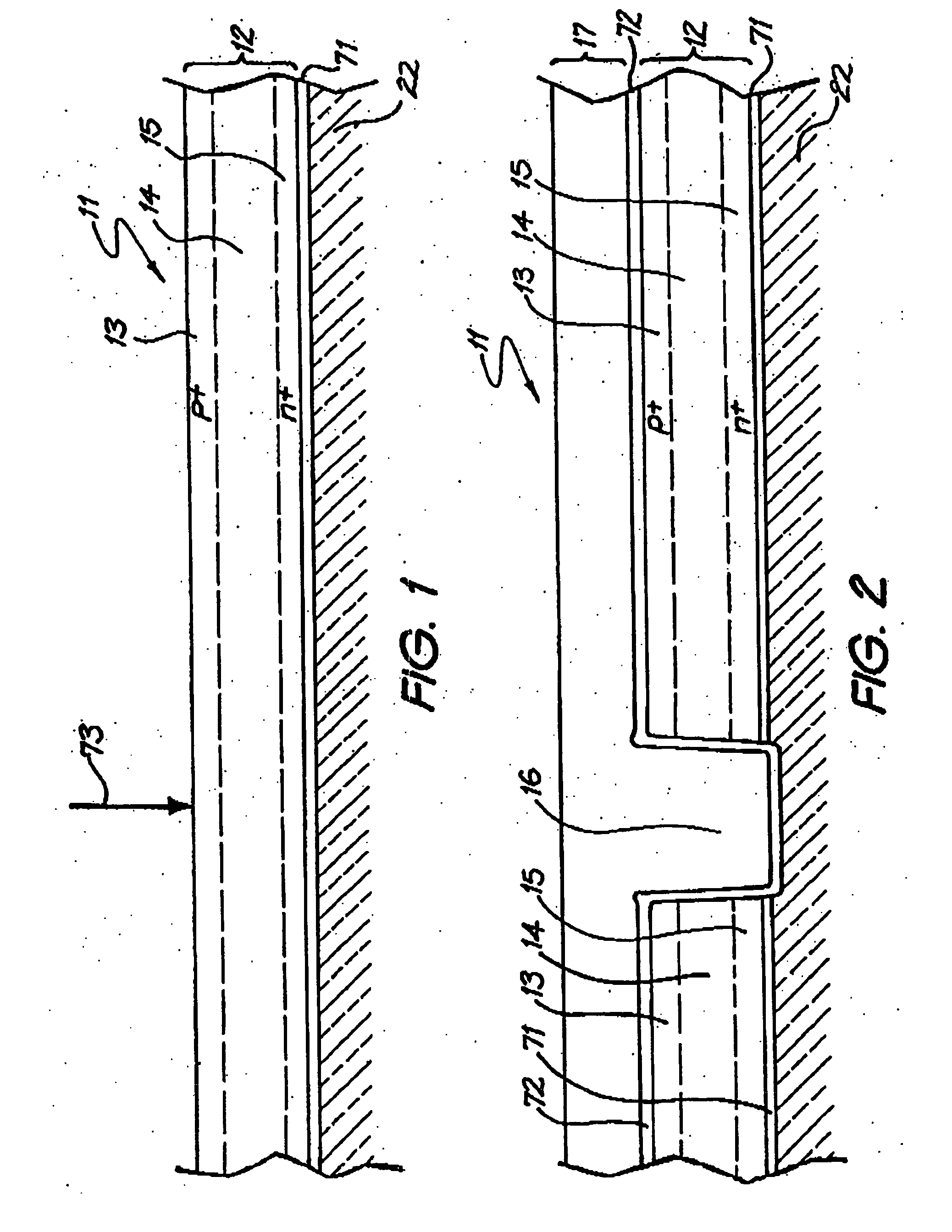
[0028] Referring to the drawings, FIG. 1 illustrates a part of a semiconductor structure 11 which is a precursor to the photovoltaic device fabrication process described below. The semiconductor structure 11 is formed as a thin semiconductor film applied to a substrate 22 in the form of a glass sheet to which a thin silicon nitride anti-reflection coating 71 has been applied. The anti-reflection coating 71 has a thickness of 80 nm. For optimal performance, the thin semiconductor film comprises a thin polycrystalline silicon film 12 formed with a total thickness in the range of 1 to 2 μm and preferably 1.6 μm. The polycrystalline silicon film 12 has an upper p+ type region 13 which is 60 nm thick, a lower n+ type region 15 which is 40 nm thick, and a 1.5 μm thick intrinsic or lightly p type doped region 14 separating the p+ and n+ type regions. The sheet resistance in both + type and p+ type layers is preferably between 400 and 2500 Ω / □, with no more than 2×1014 cm−2 boron in total. ...
PUM
 Abstract
Description
Claims
Application Information
 - R&D
- Intellectual Property
- Life Sciences
- Materials
- Tech Scout
- Unparalleled Data Quality
- Higher Quality Content
- 60% Fewer Hallucinations
Browse by: Latest US Patents, China's latest patents, Technical Efficacy Thesaurus, Application Domain, Technology Topic, Popular Technical Reports.
© 2025 PatSnap. All rights reserved.Legal|Privacy policy|Modern Slavery Act Transparency Statement|Sitemap|About US| Contact US: help@patsnap.com


