
Semiconductor device fabrication methods employing substantially planar buffer material layers to improve the planarity of subsequent planarazation processes

a semiconductor device and buffer material technology, applied in the direction of capacitors, electrical appliances, basic electric elements, etc., can solve the problems that the surface of the material or materials that fill the recesses and may cover the surface of the semiconductor device structure has not yet been chemically-mechanically planarized, and achieves the effect of reducing the depth of material

Inactive Publication Date: 2007-01-04
WHITMAN JOHN +1
View PDF28 Cites 4 Cited by
  • Summary
  • Abstract
  • Description
  • Claims
  • Application Information

AI Technical Summary

Problems solved by technology

The surfaces of the material or materials that fill the recesses and that may cover the surfaces of the semiconductor device structures have not, however, been chemical-mechanical planarized to achieve the reduced depth of material outside of the recesses.

Method used


Image

  • Semiconductor device fabrication methods employing substantially planar buffer material layers to improve the planarity of subsequent planarazation processes
  • Semiconductor device fabrication methods employing substantially planar buffer material layers to improve the planarity of subsequent planarazation processes
  • Semiconductor device fabrication methods employing substantially planar buffer material layers to improve the planarity of subsequent planarazation processes

Examples


Embodiment Construction

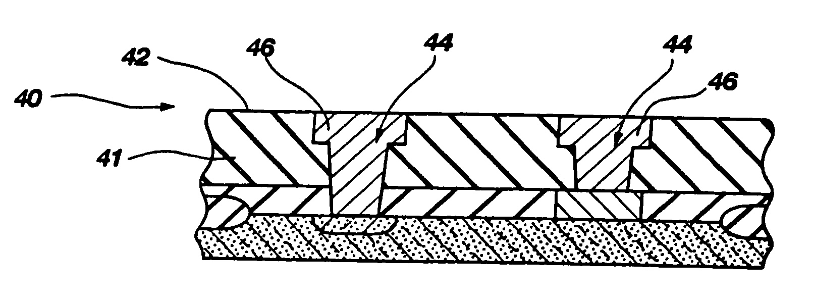
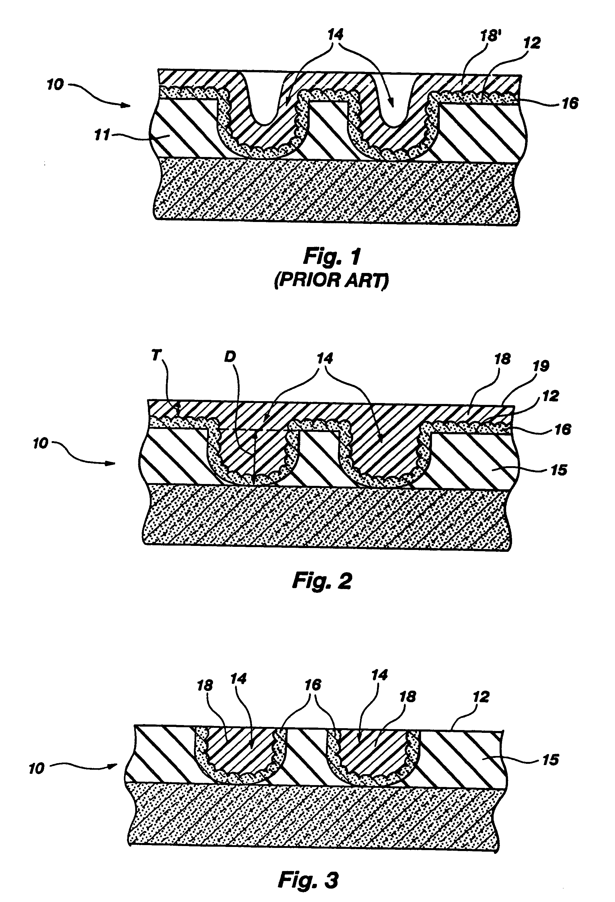
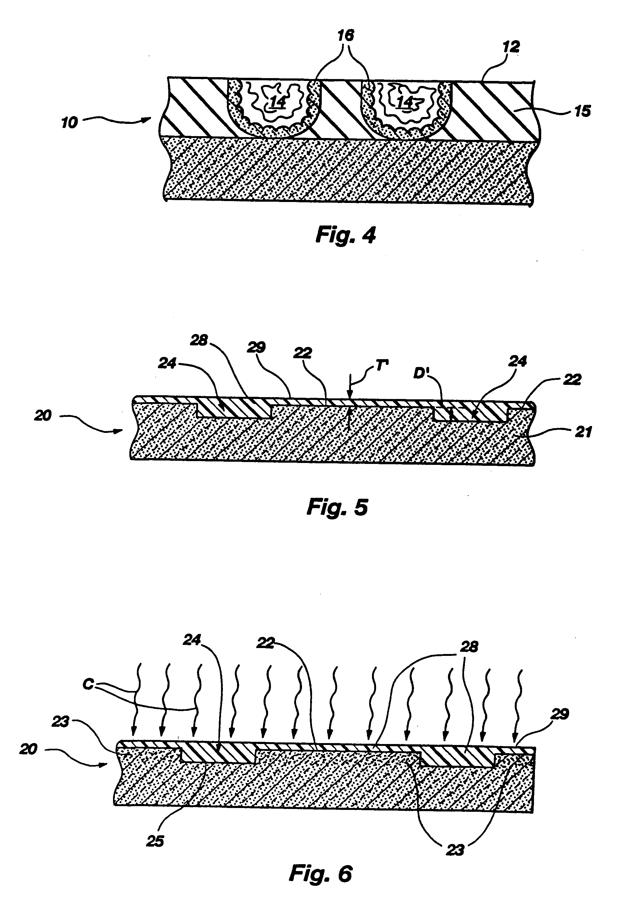
[0041] With reference to FIG. 2, a semiconductor device structure, in this case a stacked capacitor structure 10, incorporating teachings of the present invention is illustrated. Stacked capacitor structure 10 includes a surface 12 with containers 14 recessed, or formed, in surface 12. As illustrated, surface 12 and containers 14 are lined with a layer 16 of conductively doped hemispherical grain silicon. Stacked capacitor structure 10 also includes a mask layer 18 of a polymer material (e.g., polyimide or photoresist) disposed over layer 16. Mask layer 18 substantially fills containers 14 and has a substantially planar exposed surface 19. The thickness T of portions of mask layer 18 overlying surface 12 is less than the depth D of containers 14 and, preferably, is less than about half of depth D.

[0042] Stacked capacitor structure 10, including the conductively doped hemispherical grain silicon layer 16 thereof, may be fabricated by known processes, such as those disclosed in U.S. ...


PUM

PropertyMeasurementUnit
temperatureaaaaaaaaaa
stressaaaaaaaaaa
electrical insulatoraaaaaaaaaa

Abstract

A method for fabricating a semiconductor device structure includes applying a stress buffer material onto a semiconductor device structure and spreading the stress buffer material. When the stress buffer material is spread, it substantially fills recesses formed in a surface of the semiconductor device structure and imparts the stress buffer material with a substantially planar surface. The thickness of the stress buffer material covering the surface of the semiconductor device structure may be less than the depths of the recesses. The surface may remain substantially uncovered by the material.

Description

CROSS-REFERENCE TO RELATED APPLICATION [0001] This application is a divisional of application Ser. No. 09 / 542,783, filed Apr. 4, 2000, pending.BACKGROUND OF THE INVENTION [0002] 1. Field of the Invention [0003] The present invention relates to methods for filling containers, trenches, or other recesses of semiconductor device structures during fabrication thereof. Particularly, the present invention relates to the use of spin coating techniques to fill containers, trenches, and other recesses of semiconductor device structures. As a specific example, the present invention relates to a method for masking hemispherical grain (HSG) silicon-lined containers of a stacked capacitor structure to facilitate removal of HSG silicon from the surface of a semiconductor device structure including the stacked capacitor structure. [0004] 2. Background of Related Art [0005] Conventionally, spin-on processes have been used to apply substantially planar layers of material to the surfaces of semicondu...

Claims


Application Information

Patent Timeline
Patent Type & Authority Applications(United States)
IPC IPC(8): H01L21/302H01L21/31H01L21/02H01L21/762H01L21/768
CPCH01L21/76232H01L28/84H01L21/7684
Inventor WHITMAN, JOHNDAVLIN, JOHN
Owner WHITMAN JOHN
Learn More