Chemical solution application apparatus and chemical solution application method
a chemical solution and application apparatus technology, applied in the direction of photomechanical apparatus, coatings, instruments, etc., can solve the problems of wasting discharge materials, discharge point patterns cannot be selected, application cannot be even over a substrate, etc., to achieve the effect of reducing waste, improving efficiency, and drastically improving the use efficiency of resists
- Summary
- Abstract
- Description
- Claims
- Application Information
AI Technical Summary
Benefits of technology
Problems solved by technology
Method used
Image
Examples
embodiment modes
[0041] Although the present invention will be described by way of embodiment modes with reference to the accompanying drawings, it is to be understood that various changes and modifications will be apparent to those skilled in the art. Therefore, unless such changes and modifications depart from the scope of the invention, they should be construed as being included therein.
embodiment mode 1
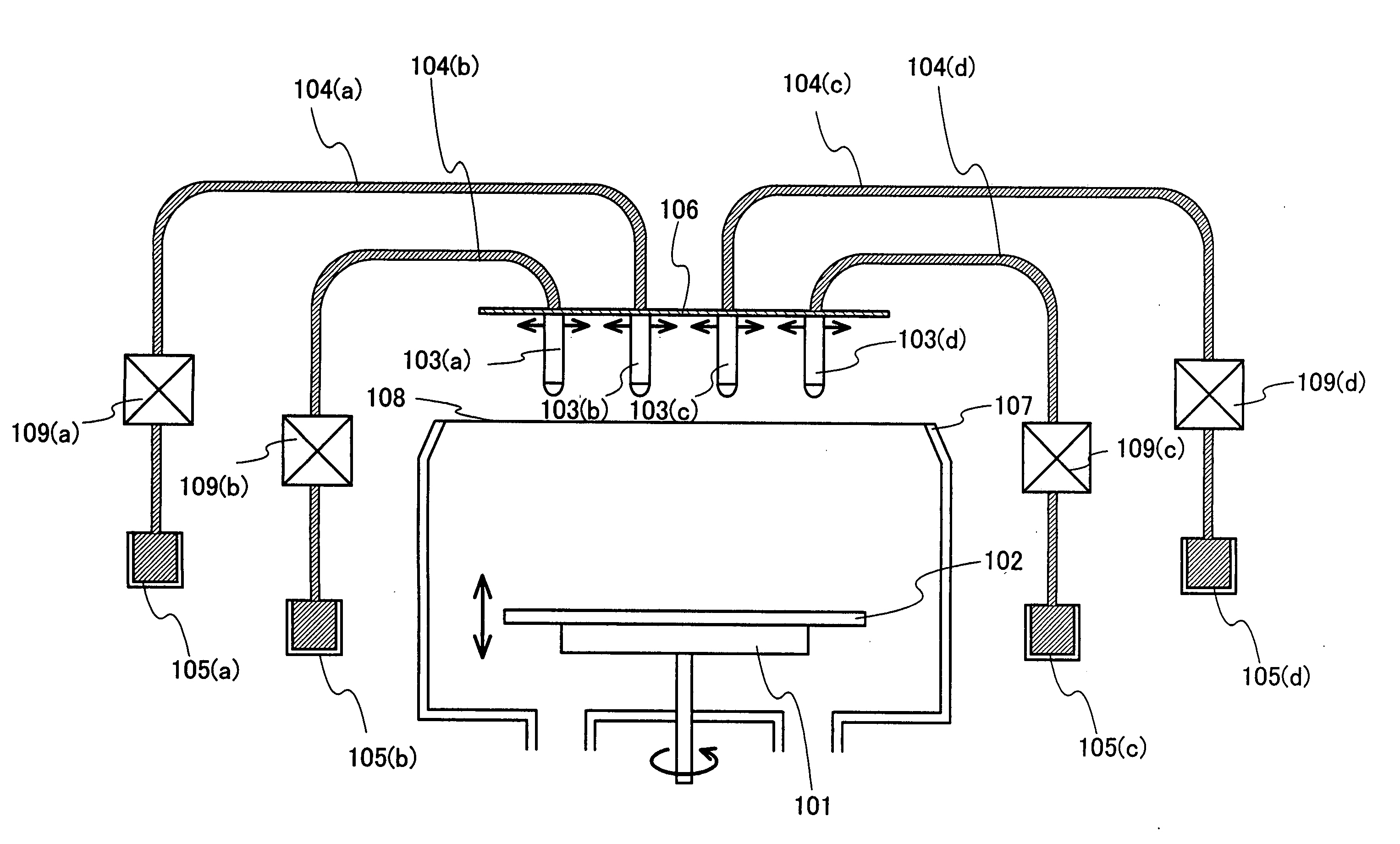
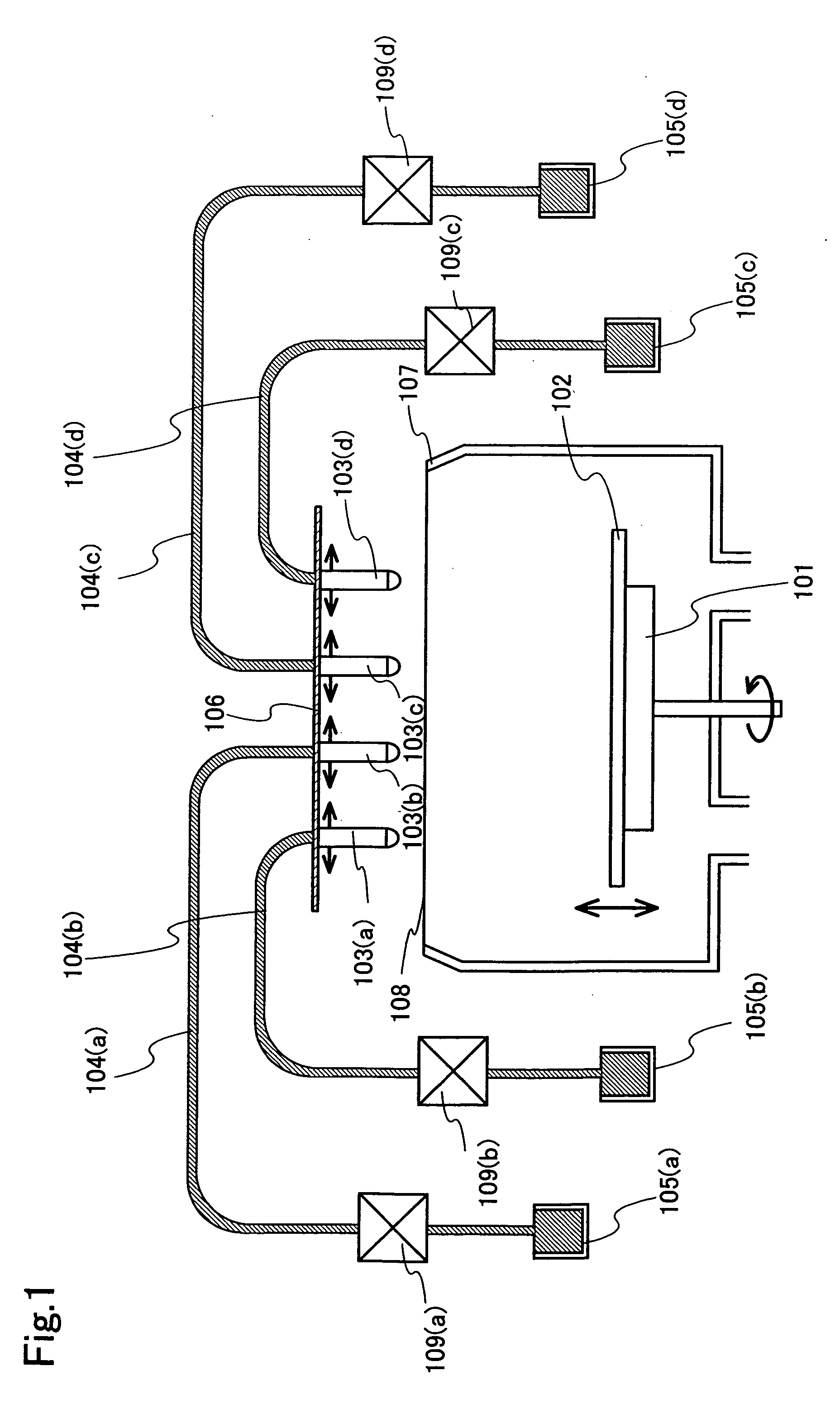
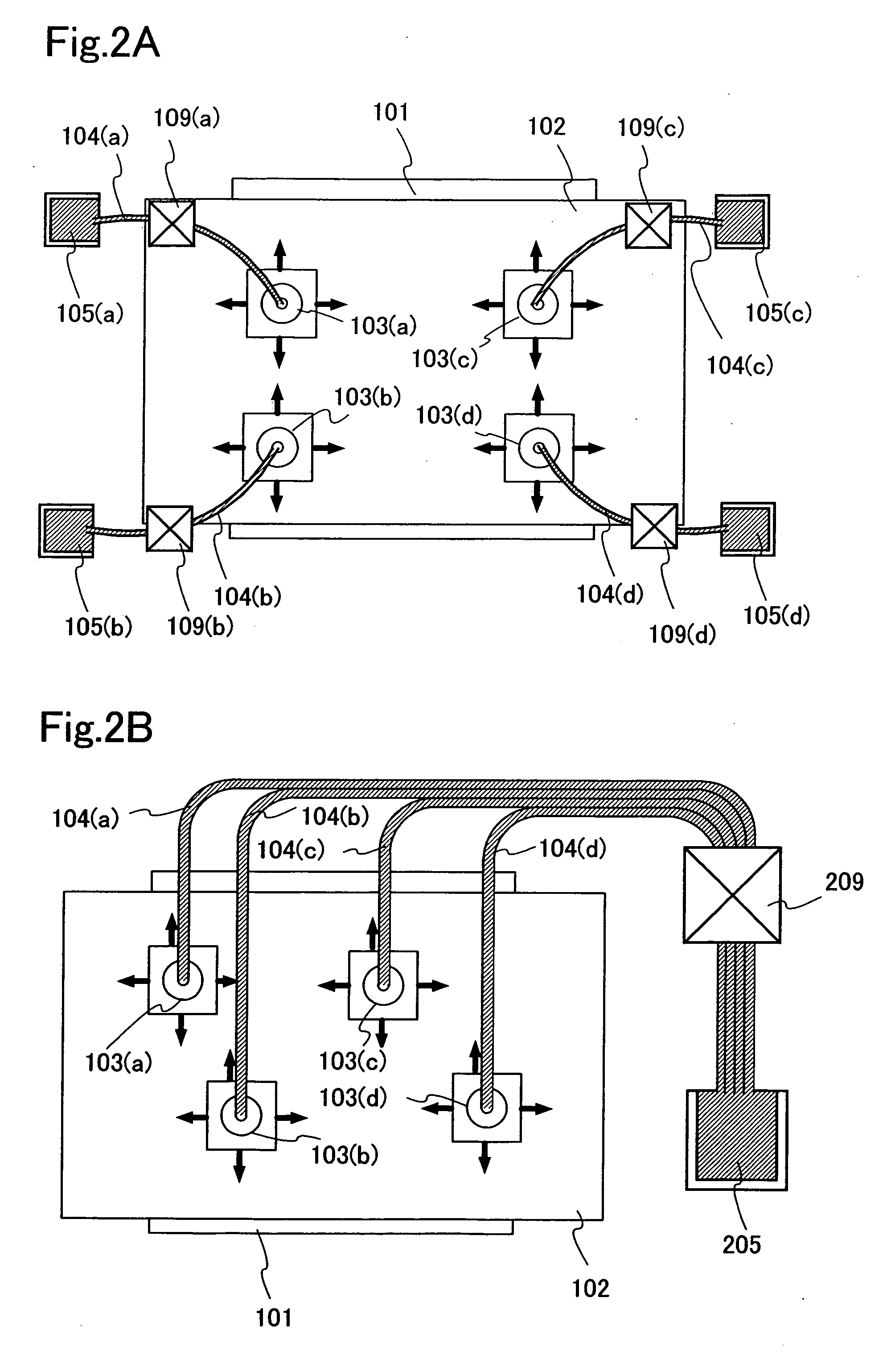
[0042] First, a chemical solution application apparatus equipped with a plurality of mobile nozzles is described using FIG. 1 and FIGS. 2A and 2B. FIG. 1 is a side view of a chemical solution application apparatus of the present invention, and FIGS. 2A and 2B are top views. A substrate 102 is set over a suction stage 101 (also called a rotation supporting board or turntable). Also, a plurality of mobile nozzles 103(a) to (d) are fixed on a guide rail 106 (abbreviated in FIGS. 2A and 2B). Each of the nozzles 103(a) to (d) can change directions along an x axis, a y axis, and a z axis, and are connected to chemical solution pumping portions (tanks) 105(a) to (d) through pipings 104(a) to (d). Between the plurality of nozzles 103 and the tanks 105, chemical solution discharge control mechanisms (also called discharge controlling means or control portions) 109(a) to (d) are connected to control them. Further, each of the tanks 105(a) to (d) which has received a signal from the chemical s...
embodiment mode 2
[0051] This embodiment mode is described using FIGS. 7A to 15. More specifically, a manufacturing method of a display device (which means a liquid crystal display device herein) to which the present invention is applied is described. First, a manufacturing method of a display device including a channel-etch type thin film transistor, to which the present invention is applied is described. Figures A of FIGS. 7 to 9 and FIGS. 11 to 13 each show a top view of a display device pixel portion, and the figures B of FIGS. 7 to 9 and FIGS. 11 to 13 each show a cross-sectional view of the figures A of FIGS. 7 to 9 and FIG. 11 along lines G-H.
[0052] Over a substrate 700, a base film 701 is formed as a base pretreatment. For the substrate 700, a glass substrate made from barium borosilicate glass, alumino borosilicate glass, or the like; a quartz substrate; a silicon substrate; a metal substrate; a stainless steel substrate; or a plastic substrate having heat resistance that can resist a treat...
PUM
 Abstract
Description
Claims
Application Information
 - R&D
- Intellectual Property
- Life Sciences
- Materials
- Tech Scout
- Unparalleled Data Quality
- Higher Quality Content
- 60% Fewer Hallucinations
Browse by: Latest US Patents, China's latest patents, Technical Efficacy Thesaurus, Application Domain, Technology Topic, Popular Technical Reports.
© 2025 PatSnap. All rights reserved.Legal|Privacy policy|Modern Slavery Act Transparency Statement|Sitemap|About US| Contact US: help@patsnap.com


