
Thin planar switches and their applications

Inactive Publication Date: 2006-11-09
CITALIA LTD
View PDF2 Cites 76 Cited by
  • Summary
  • Abstract
  • Description
  • Claims
  • Application Information

AI Technical Summary

Benefits of technology

[0045] A preferred method of opening any of the above-mentioned switches again is by the application of physical stress to the device, either in the form of pressure, or in the form of bending, or by the application of heat. Preferred methods of switching off the device thus include the application of mechanical shock, stress or vibration. One preferred method of applying these in a controlled manner is by the use of a piezoelectric chip or layer attached to the device to introduce a level of stress into the switching material. Alternatively and preferably, the piezoelectric material can be mixed into the switching material. According to yet another preferred embodiment of the present invention, the addition of an elastomer to the switching material facilitates its reversal to the open state much more rapidly. According to yet more preferred embodiments, the use of a viscous or a gel-like insulating matrix material, also facilitates the switch reversal to the open state.
[0084] In accordance with a first preferred embodiment of a color display according to the present invention, the latching optical switch of the present invention are utilized to construct new forms of color displays, based on a subtractive system of color generation, rather than the additive system used in current displays. According to this preferred embodiment, the screen is made up of three layers of pixelated latched optical switches, according to the present invention, arranged in tandem, one on top of the other. One of the layers has its conductive metallic dispersion colored cyan, the second, magenta, and the third yellow. These colors are those conventionally used in subtractive color printing or display processes, as is well known in the art. When no voltage is applied across a pixel in the first layer, the color of the pixel is that of the colored metal namely cyan. Application to the electrodes of that pixel of an increasing voltage, causes the pixel to change from its non-transparent cyan color to become virtually fully transparent, if the switching layer has been correctly constructed, and the materials correctly selected, without too high or low a concentration of metal. Likewise for the second layer, any pixel can be switched from a fully opaque magenta to virtually transparent, and likewise for the yellow, third layer. Since the layers are in series, the screen thus has the property that any pixel can be switched from virtually complete transparency to any combination of the cyan-magenta-yellow color combination, thus providing a reflective display which emulates the subtractive color printing process.
[0101] In accordance with this method, the display panel preferably may have a resolution approximately three times better than a corresponding additive display, and an optical efficiency approximately three times better than a corresponding additive display.
[0102] Furthermore, in accordance with yet another preferred embodiment of the present invention, there is provided a method of improving the resolution of a display panel including three sets of pixelated filters of different colors, including the steps of selecting the colors to be a subtractive color set, disposing the filters one on top of the other, such that at least one set of corresponding pixels of each of the filters are superposed, and activating the set of superposed pixels in a subtractive mode.
[0103] There is further provided in accordance with still another preferred embodiment of the present invention a method of improving the optical efficiency of a display panel including three sets of pixelated filters of different colors, including the steps of selecting the colors to be a subtractive color set, disposing the filters one on top of the other, such that at least one set of corresponding pixels of each of the filters are superposed, and activating the set of superposed pixels in a subtractive mode.
[0104] The pressure sensitive properties of the above described latching switch device, whereby application of pressure is operative to open a switch element which is latched close, as described above, enables the devices of the present invention to be used, according to further preferred embodiments of the present invention, as a novel touch panel or touch screen. The touch panel can preferably be used like conventional touch panels, as a separate unit, mounted in front of the screen in conjunction with which it operates, but without any direct electrical association therewith. In such an embodiment, the touch panel is preferably constructed of a large latching switched panel, made up of a layer of switching material sandwiched between two thin transparent substrates. Each of the substrates has an array of transparent conductors deposited thereon, one in each orthogonal direction. The entire touch screen is held latched closed by application of an overall switching voltage. When the pressure of a touch opens one of the pixels of the touch screen, electronic circuitry which scans the entire panel row by row and column by column, by means of the two orthogonal arrays of conductors, reveals which pixel is open, and thus provides information about the location of the touch.

Problems solved by technology

However, it would appear from the reported behavior that the switching effect is not always reproducible, and no details of any methods of application are given, nor are the applicants aware of any apparent commercial applications developed from these devices.
The bi-stable latching switches described in the prior art which have found commercial application are generally solid state semiconductor devices, such as four leg p-n-p-n devices, and, being multi-layered, are generally relatively complex and hence costly to manufacture and may have low yields.
Such arrays are complex and expensive, thus making the cost of such active matrix displays comparatively high.
Ferroelectric-based latching switches and liquid crystals are also used in the display industry, but their cost is also high.
However, the performance of passive liquid crystal displays (LCD's) is noticeably inferior to that of active matrix LCD's in a number of areas.
The primary reason for the inferior performance of passive LCD's in flat panel applications, where multiple lines need to be displayed, is a result of the method whereby their pixels are addressed by multiplexing.
However, in order to achieve such contrast levels when multiplexing is used, an LCD material having a much steeper characteristic than those of currently available technologies, would be required, and such a material is currently unavailable, with the exception of Ferroelectric liquid crystal devices, which are expensive, lack gray scale and are difficult to fabricate.
Reading such a passive display with more than about 400 rows using currently available materials is difficult, making such passive displays unsuitable for high resolution large screen devices, such as computer screens.
For this reason, passive type displays have been limited to simpler displays, such as hand held type displays, where the maximum number of rows driven is of the order of only 100-200, and the contrast can be compromised.
In such applications, the high cost of using active matrix TFT displays in order to achieve higher resolution or contrast, is not warranted.
Unfortunately, this configuration is wasteful, both in terms of light utilization, and in terms of space utilization.
Touch screens are used in many current computer-based information systems, especially those whose operation is, by their nature, very user-interface intensive, such as PDAs, automatic cash machines, information-kiosks, computer-based training devices, and computer systems for disabled users who have a difficulty in operating a mouse or keyboard.
Despite being so common, the cost of these touch-sensitive devices has remained high in comparison to conventional keyboard interface equivalents.
The nature of the material used for such curved applications limits the light throughput.
The antiglare option minimizes glare, but results in a slightly diffuse image light throughput.
However, because of the nature of its operation, a capacitive touch-screen cannot generally be activated while wearing most types of gloves, which are non-conductive.
The disadvantage of infra-red touch screens is that the bezel system that houses the transmitters and detectors can impose design constraints on operator interface products.
When the user touches the glass surface, the water content of the user's finger in contact with the glass surface absorbs some of the ultrasonic energy, thus damping the acoustic wave.
Besides the specific disadvantages mentioned above, and those known generally, which are specific to one or another of the touch screen technologies, all of the technologies have two common disadvantages: (i) They all require the use of an additional screen, and of special controllers and drivers for the touch screen panel, thereby increasing the cost of the touch-screen display.
(ii) These additional screens are placed in front of the display, thus lowering its light efficiency.

Method used


Image

  • Thin planar switches and their applications
  • Thin planar switches and their applications
  • Thin planar switches and their applications

Examples


Embodiment Construction

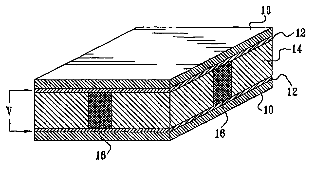
[0132] Reference is now made to FIG. 1, which schematically illustrates a latched planar switch, constructed and operative according to a preferred embodiment of the present invention. The device is composed of a pair of substrates 10, preferably made of glass, quartz, polyethylene, polyester, or a similar thin insulating material in the form of a sheet, between which is sandwiched a layer of switching material 14. The switching material 14, according to another preferred embodiment of the present invention, is a metal loaded epoxy, made by adding a suspension of metallic silver, iron, gold, copper, zinc, aluminum or another similar metal to an epoxy mixture before curing. The epoxy can preferably be Epon Resin 828, supplied by the Shell Chemical Company of Houston, Tex., USA, with Cap-cure 3-800 hardener. The chemical composition of this, and of many other suitable epoxy resins, is bisphenot A / epichlorohydrin with a trimercaptan cross-lining catalyst. However, the invention can als...


PUM


Abstract

A novel thin planar latching switch device, generally based on a layer of polymeric switching materials sandwiched between two electrical planar conductors operative as electrodes. The device behaves as a bi-stable switch. Furthermore, the switch device generally shows a memory effect. In the open state, when no voltage is applied to the electrodes, the switching material is effectively an insulator. When an electric field greater than a certain threshold level is applied to the switching material, the material becomes more conductive, and the device thus essentially becomes a closed switch. Applications of such switching devices are described for use in flat panel displays, generally based on liquid crystals, in high efficiency color displays, and in touch screens.

Description

FIELD OF THE INVENTION [0001] The present invention relates to the field of latched planar solid state optical and electronic switching devices with a memory for the state to which they are switched, especially for use in planar switching applications, in flat panel displays, in high efficiency color displays, and in touch screen applications. BACKGROUND OF THE INVENTION [0002] In various applications, it is desired to have a switching device with latching properties, such that when it is turned on, it remains latched in the closed state, until switched off again by means of a disenabling function. Such switches generally have bi-stable behavior, i.e. they have two preferentially favored switched conditions, open and closed, and have little tendency to be found between those two favored conditions. They also generally have non-ohmic behavior, i.e., they are nonlinear electronic devices, even before reaching their switching threshold. One of the earliest types of switching device wit...

Claims


Application Information

Patent Timeline
IPC IPC(8): G02F1/136G02F1/133G09F9/30G02F1/1365G06F3/033G06F3/048H01C7/02H01C7/10H01L45/00H01L49/02H03K17/96
CPCG02F1/13338G02F1/1365G02F2202/022G06F3/0488H01C7/027H01L45/1608H01L45/04H03K17/964H01L45/1233H01L45/14H01C7/1006H10N70/20H10N70/826H10N70/881H10N70/021
Inventor KUTSCHER, TUVIA D.MARCO, DORONTURLIUC, GADIGOREN, TOVITEILAT, AMIR
Owner CITALIA LTD
Learn More