
Thermoelectric semiconductor material, thermoelectric semiconductor element therefrom, thermoelectric module including thermoelectric semiconductor element and process for producing these

a technology of thermoelectric semiconductor elements and semiconductor materials, which is applied in the direction of thermoelectric device junction materials, thermoelectric device manufacturing/treatment, thermoelectric devices, etc., can solve the problems of difficult to overcome problems, few methods for still increasing performance, and insufficient mechanical strength of thermoelectric semiconductor materials, etc., to achieve enhanced thermoelectric performance, enhanced thermoelectric performance, and uniform deformation rate

Inactive Publication Date: 2006-11-02
IHI CORP
View PDF4 Cites 25 Cited by
  • Summary
  • Abstract
  • Description
  • Claims
  • Application Information

AI Technical Summary

Benefits of technology

[0031] Therefore, an object of the present invention is to provide a thermoelectric semiconductor material having excellent crystalline orientation in the texture, reduced oxygen concentration, and enhanced thermoelectric performance, as well as to provide a thermoelectric semiconductor element using such a thermoelectric semiconductor material, a thermoelectric module using such a thermoelectric element, and manufacturing methods for same.

Problems solved by technology

There is a problem, however, in that the mechanical strength of a thermoelectric semiconductor material cannot be sufficiently enhanced, even when the thermoelectric semiconductor material is manufactured by plastically deforming an ingot of a thermoelectric semiconductor raw alloy, as shown in Patent Document 1.
At present, it is difficult to overcome the problem in which a single-crystal or directionally solidified ingot easily cracks along the cleavage plane of the material.
Even though the orientation of the crystals is uniform, there are few methods for still increasing performance, because the manufacturing methods are limited.
However, the size of the powder particles determine the diameter of the crystal grains in the powder of the ingot, and there is a limit to the miniaturization of the cry grains.
Therefore, the thermoelectric semiconductor material is disadvantageous in reducing thermal conductivity (a) and the thermoelectric performance cannot be significantly enhanced.
In addition, since the powder is sintered in a state in which each powder particles are randomly oriented, by the plastic deformation of the sintered body having such disordered crystalline orientation, it is difficult to enhance the crystalline orientation of a tenure of thermoelectric semiconductor material.
However, the grain boundaries inevitably exist in a polycrystalline body.
Therefore, at present, it is difficult to increase electric conductivity and to reduce thermal conductivity at the same time.
In addition, there is a problem in that the electric resistance is lowered in the vicinity of grain boundaries where the impurities are concentrated, whereas inside of the grains which mainly make up the volume are converted to semiconductors, and thus, electric resistance increases.
However, Patent Document 12 does not show any concrete processes for manufacturing a thermoelectric semiconductor material by solidifying and forming a raw thermoelectric semiconductor material in foil or powder form that has been manufactured by using a rotational roll of which the circumferential velocity has been set as described above.
Therefore, the technique includes a problem in that the added amount of Ag must be strictly adjusted, and also includes a problem of age deterioration.
Therefore, there is a problem in which the crystal orientation of the layered raw thermoelectric semiconductor material is disordered when pressure is applied in the direction parallel to the direction of the film thickness.
However, the direction of c-axis of the hexagonal structure in each crystal grain cannot be uniformly oriented.
Even when such additional operations are carried out, it is difficult to reduce influence of oxidization.
In addition, since each of the above-described raw materials has fine grain size, it is difficult to increase density of the material during sintering.
When a powder is sintered, reduction of density depends on the grain size, but is limited to approximately 95%.

Method used


Image

  • Thermoelectric semiconductor material, thermoelectric semiconductor element therefrom, thermoelectric module including thermoelectric semiconductor element and process for producing these
  • Thermoelectric semiconductor material, thermoelectric semiconductor element therefrom, thermoelectric module including thermoelectric semiconductor element and process for producing these
  • Thermoelectric semiconductor material, thermoelectric semiconductor element therefrom, thermoelectric module including thermoelectric semiconductor element and process for producing these

Examples


example

[0179] A thermoelectric module 1a was manufactured by forming a PN element pair of P type and N type thermoelectric semiconductor elements 2a and 3a manufactured by a manufacturing method for a thermoelectric semiconductor element of the present invention. The thermoelectric performance of the module was compared with that of a thermoelectric module manufactured in accordance with another method.

[0180] As a result, the Figure-of-Merit, shown by solid circle ● and open circle o in FIG. 26, were obtained as the thermoelectric performance of thermoelectric module 1a manufactured in accordance with the present invention.

[0181] The result indicates, it was found that high thermoelectric performance is gained according to the invention.

[0182] As a result, thermoelectric module of the present invention indicates high thermoelectric performance in comparison with a case in which a P type thermoelectric semiconductor element and an N type thermoelectric semiconductor element are both manu...


PUM

PropertyMeasurementUnit
Temperatureaaaaaaaaaa
Fractionaaaaaaaaaa

Abstract

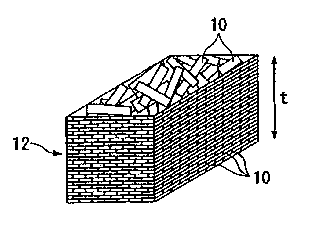
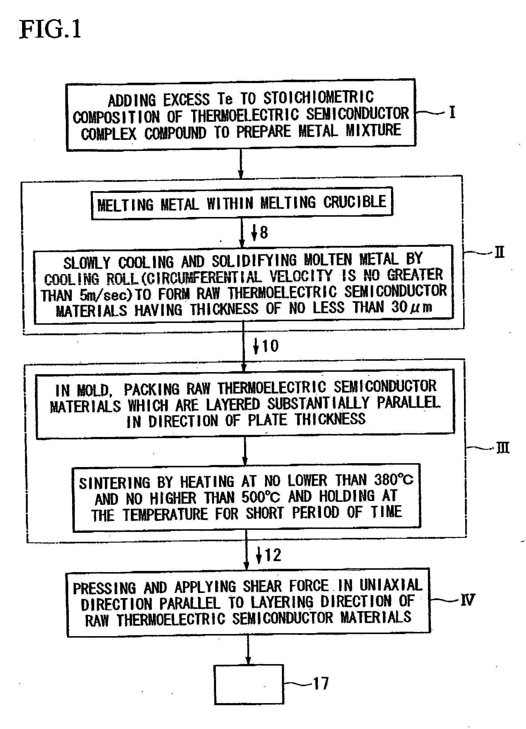
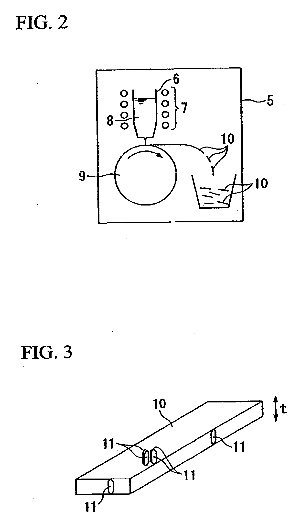
A metal mixture is prepared, in which an excess amount of Te is added to a (Bi—Sb)2Te3 based composition. After melting the metal mixture, the molten metal is solidified on a surface of a cooling roll of which the circumferential velocity is no higher than 5 m / sec, so as to have a thickness of no less than 30 μm. Thus, a plate shaped raw thermoelectric semiconductor materials 10 are manufactured, in which Te rich phases are microscopically dispersed in complex compound semiconductor phases, and extending directions of C face of most of crystal grains are uniformly oriented. The raw thermoelectric semiconductor materials 10 are layered in the direction of the plate thickness. And the layered body is solidified and formed to form a compact 12. After that, the compact 12 is plastically deformed in such a manner that a shear force is applied in a uniaxial direction that is approximately parallel to the main layering direction of the raw thermoelectric semiconductor materials 10. As a result, a thermoelectric semiconductor 17 having crystal orientation in which extending direction of C face and the don of c-axis of the hexagonal structure are approximately aligned. As a result, the crystalline orientation is improved, and the thermoelectric Figure-of-Merit is increased.

Description

TECHNICAL FIELD [0001] The present invention relates to a thermoelectric semiconductor material as well as to a thermoelectric semiconductor element, a thermoelectric module, and manufacturing method for same that are utilized for thermoelectric cooling, thermoelectric heating, thermoelectric power generation or the like. BACKGROUND ART [0002] Devices for carrying out thermoelectric cooling, thermoelectric heating and thermoelectric power generation using the thermoelectric properties of a thermoelectric semiconductor generally have a basic configuration where a plurality of thermoelectric modules 1 are aligned and connected in series, as shown schematically in the example of FIG. 27. In each of the thermoelectric modules 1, a PN element pair is formed by joining a P type thermoelectric semiconductor element 2 to an N type thermoelectric semiconductor element 3 via a metal electrode 4. [0003] One type of thermoelectric semiconductor that forms above described thermoelectric semicond...

Claims


Application Information

Patent Timeline
IPC IPC(8): H01L35/00B22D11/06C22C28/00H01L35/16H01L35/34
CPCB22D11/0611H01L35/34H01L35/16H10N10/852H10N10/01
Inventor OTA, TOSHINORIYOSHIZAWA, HIROKIFUJITA, KOUITIIMAI, ISAOTOSHO, TSUYOSHINISHIIKE, UJIHIRO
Owner IHI CORP
Learn More