
Semiconductor memory device and method of manufacturing the same

a memory device and semiconductor technology, applied in the direction of semiconductor devices, electrical devices, transistors, etc., can solve the problems of decrease of electric capacitance, and faulty operation of memory devices

Inactive Publication Date: 2006-10-26
KK TOSHIBA
View PDF1 Cites 74 Cited by
  • Summary
  • Abstract
  • Description
  • Claims
  • Application Information

AI Technical Summary

Benefits of technology

[0011] A semiconductor memory device according to a first aspect of the present invention comprises a semiconductor substrate, a tunnel insulating film formed on the semiconductor substrate, a floating gate electrode formed on the tunnel insulating film, and having a first side-surface portion positioned in an upper portion and a second side-surface portion positioned below the first side-surface portion, an element isolation trench formed in the semiconductor substrate to be adjacent to the floating gate electrode, a first element isolation insulating film formed along a side surface and bottom surface of the element isolation trench from the second side-surface portion of the floating gate electrode, a second element

Problems solved by technology

This decreases the electric capacitance of the interelectrode insulating film 208, and causes faulty operations of the memory device.
However, the following problems arise if the silicon nitride layers 231 and 232 are formed by using CVD or thermal nitriding.
This decreases the capacitance of the interelectrode insulating film 208 and increases the parasitic capacitance between the adjacent cells, so the memory device suffers faulty operation.
Since this depletes the buried portion of the control gate electrode CG, the memory device suffers faulty operation.
This decreases the breakdown voltage between the substrate 201 and control gate electrode CG, so the memory device suffers faulty operation.
These problems are significant when the depth P, width Q, and distance R are approximately 100 nm or less.
Since this degrades the quality of a tunnel oxide film 202, the reliability of the memory device is also degraded.

Method used


Image

  • Semiconductor memory device and method of manufacturing the same
  • Semiconductor memory device and method of manufacturing the same
  • Semiconductor memory device and method of manufacturing the same

Examples


first embodiment

[0024] In a first embodiment, a radical nitride film is formed by radical nitriding on an interelectrode insulating film between a floating gate electrode and control gate electrode.

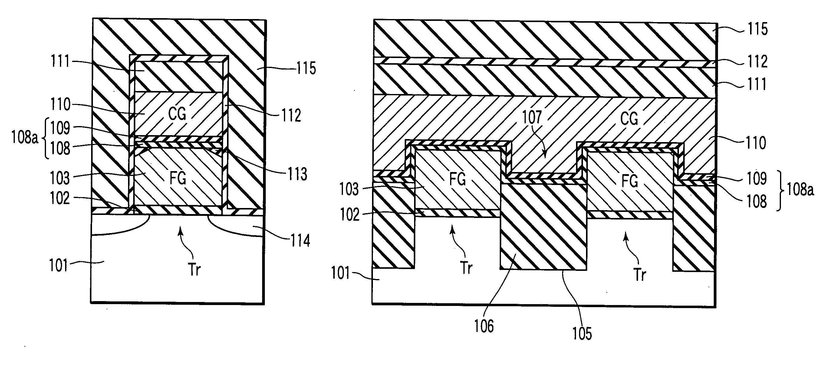
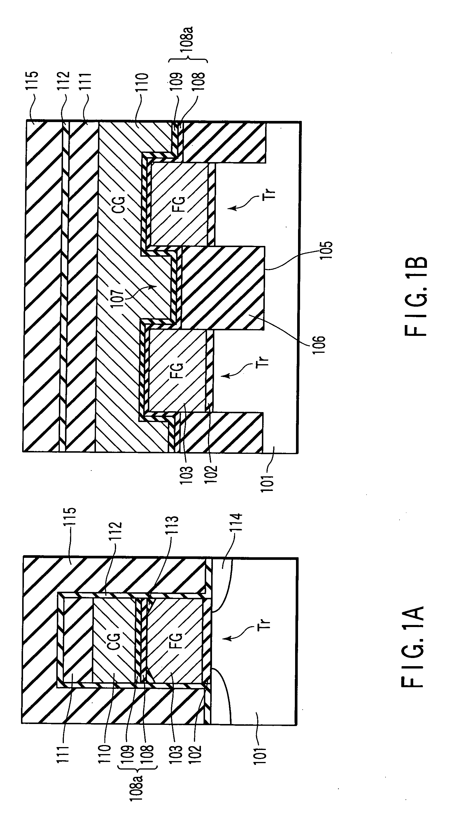
[0025]FIGS. 1A and 1B are sectional views of a nonvolatile semiconductor memory device according to the first embodiment of the present invention. FIG. 1A is a sectional view in the bit line direction (channel length direction), and FIG. 1B is a sectional view in the word line direction (channel width direction). This nonvolatile semiconductor memory device according to the first embodiment will be explained below.

[0026] As shown in FIGS. 1A and 1B, floating gate electrodes FG are formed on a silicon substrate 101 via a tunnel oxide film 102, and an interelectrode insulating film 108 is formed on the floating gate electrodes FG. A radical nitride film 109 is formed on the interelectrode insulating film 108 by radical nitriding. A control gate electrode CG is formed on the radical nitride film 109, and ...

second embodiment

[0045] In the first embodiment, the radical nitride film is formed only on the interelectrode insulating film. In a second embodiment, however, radical nitride films are formed above and below an interelectrode insulating film.

[0046]FIGS. 8A and 8B are sectional views of a nonvolatile semiconductor memory device according to the second embodiment of the present invention. FIG. 8A is a sectional view in the bit line direction (channel length direction), and FIG. 8B is a sectional view in the word line direction (channel width direction). This nonvolatile semiconductor memory device according to the second embodiment will be explained below.

[0047] As shown in FIGS. 8A and 8B, the second embodiment differs from the first embodiment in that a radical nitride film 109 is formed above an interelectrode insulating film 108, and a radical nitride film 120 is formed below the interelectrode insulating film 108. When oxidation is performed to form a gate sidewall oxide film 112, therefore, ...

third embodiment

[0063] If a structure (to be referred to as an NONON structure hereinafter) having radical nitride films 109 and 120 above and below an interelectrode insulating film 108 made of an ONO film is formed when a trench 107 between adjacent floating gates FG1 and FG2 has a high aspect ratio and a narrow opening, a film thickness Tside of the radical nitride film 120 (120a) on the sidewall surfaces of the trench 107 sometimes decreases in a portion X (a side-surface portion in the lower portion of the trench 107) in the lower portion of the floating gate electrode FG1 (FG2) (FIG. 13). This is presumably because radical nitriding hardly reaches the bottom of the trench 107 to make the supply amount of radical nitriding insufficient. If this is the case, an electric charge leak between the floating gate electrode FG and a control gate electrode CG in the portion X may increase to worsen the charge retention characteristics.

[0064] To solve the above problem, a third embodiment uses means (1...


PUM


Abstract

A semiconductor memory device manufacturing method includes forming a floating gate electrode above a semiconductor substrate, forming an interelectrode insulating film above the floating gate electrode, forming a first radical nitride film on a surface of the interelectrode insulating film by first radical nitriding, and forming a control gate electrode on the first radical nitride film.

Description

CROSS-REFERENCE TO RELATED APPLICATIONS [0001] This application is based upon and claims the benefit of priority from prior Japanese Patent Application No. 2005-128232, filed Apr. 26, 2005, the entire contents of which are incorporated herein by reference. BACKGROUND OF THE INVENTION [0002] 1. Field of the Invention [0003] The present invention relates to a semiconductor memory device including a floating gate electrode and control gate electrode, and a method of manufacturing the same. [0004] 2. Description of the Related Art [0005] Conventionally, a nonvolatile semiconductor memory device including a floating gate electrode FG and control gate electrode CG has been proposed as a semiconductor memory. [0006] In this nonvolatile semiconductor memory device, as shown in FIG. 19, a floating gate electrode FG, interelectrode insulating film 208, and control gate electrode CG are processed into a desired shape, and a gate sidewall oxide film 212 is formed on the entire surface by oxidat...

Claims


Application Information

Patent Timeline
IPC IPC(8): H01L21/336H01L27/115H01L27/11521H01L29/788H01L29/792
CPCH01L27/11521H01L27/115H10B69/00H10B41/30
Inventor OZAWA, YOSHIOKAMIOKA, ISAOSHIOZAWA, JUNICHI
Owner KK TOSHIBA
Learn More