
Patterns of electrically conducting polymers and their application as electrodes or electrical contacts

a technology of electrical conductors and polymers, applied in the direction of non-metal conductors, instruments, and semiconductor/solid-state device details, etc., can solve the problems of cumbersome process and expensive tooling

Inactive Publication Date: 2006-10-26
GLOBALFOUNDRIES INC
View PDF6 Cites 22 Cited by
  • Summary
  • Abstract
  • Description
  • Claims
  • Application Information

AI Technical Summary

Benefits of technology

The present invention provides a method for creating electrically conductive polymers and patterned electrically conducting polymers with good thermal stability, no outgassing, and high optical transmission. The patterns can be used as electrical contacts for electronic devices and can exhibit good charge retention, transmission, and image sticking properties. The invention also provides methods for creating field effect transistors, liquid crystal displays, and organic light-emitting diodes with the patterned electrically conductive polymers. The patterns can be created using resist layers and metal masks. Overall, the invention provides a way to create highly functional and patterned electrically conductive polymers for various applications.

Problems solved by technology

Metals are deposited by evaporative or sputtering processes which require expensive tooling and overall are a cumbersome processes.

Method used


Image

  • Patterns of electrically conducting polymers and their application as electrodes or electrical contacts
  • Patterns of electrically conducting polymers and their application as electrodes or electrical contacts
  • Patterns of electrically conducting polymers and their application as electrodes or electrical contacts

Examples


Embodiment Construction

[0138] The present invention is directed to devices using electrically conducting polymers including substituted and unsubstituted polyanilines, polyparaphenylenes, polyparaphenylene vinylenes, polythiophenes, polypyrroles, polyfurans, polyselenophenes, polyisothianapthenes, polyphenylene sulfides, polyacetylenes, polypyridyl vinylenes, combinations thereof and blends thereof with other polymers, copolymers of the monomers thereof. It is found that these polymers can be patterned lithographically to form electrically conductive patterns which can act as electrodes or electrical contacts in various electro-optical transducers and devices. The present invention is also directed to electro-optical transducers and devices consisting of one or more electrically conductive polymer electrodes.

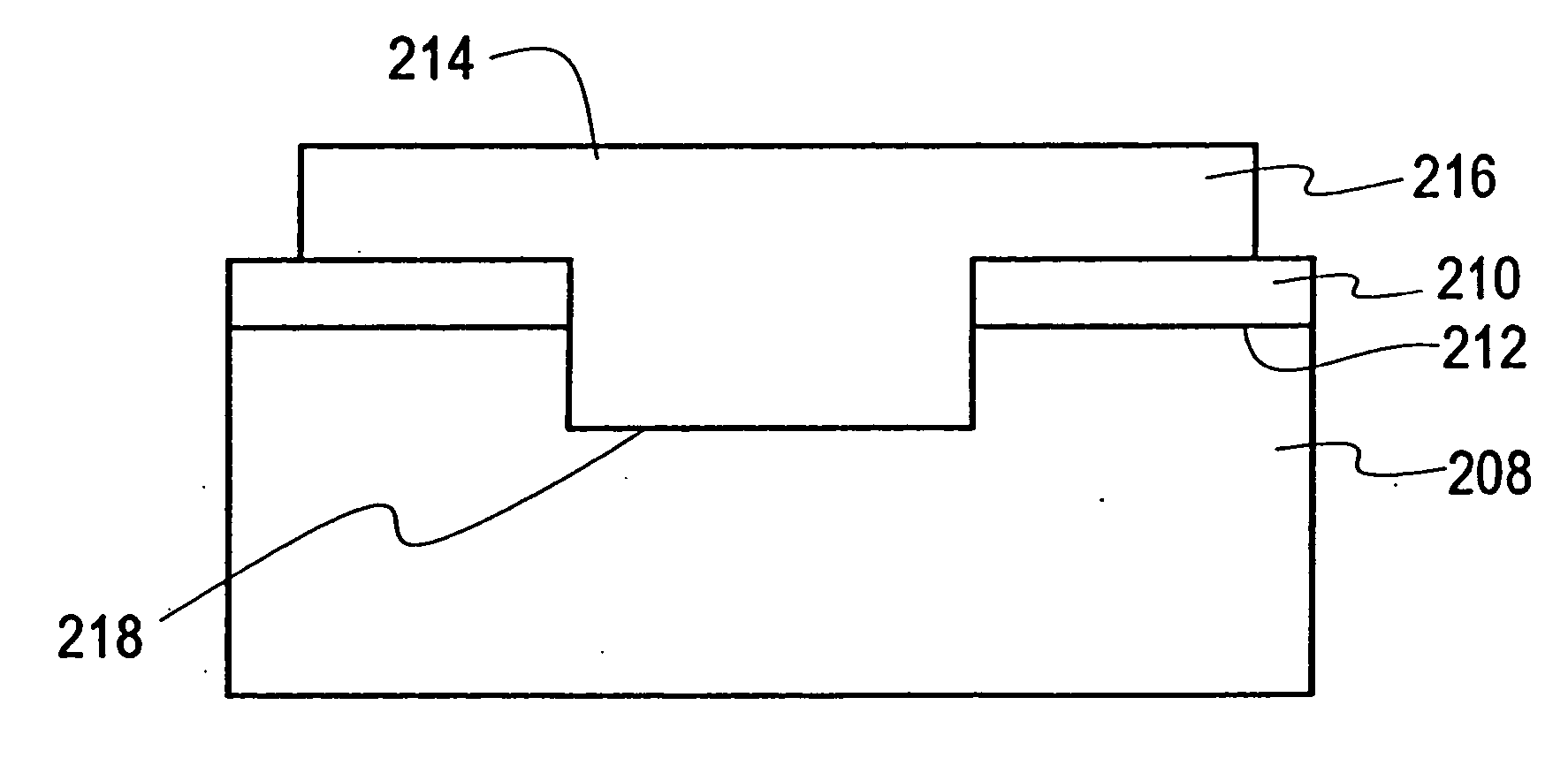
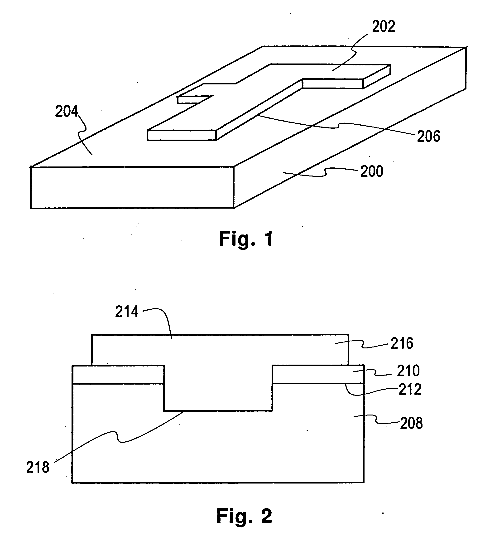
[0139]FIG. 1 schematically shows in perspective substrate 200 having patterned electrically conductive polymer 202 disposed thereon. The electrically conductive polymer 202 forms electrical contact t...


PUM

PropertyMeasurementUnit
widthaaaaaaaaaa
lengthaaaaaaaaaa
temperaturesaaaaaaaaaa

Abstract

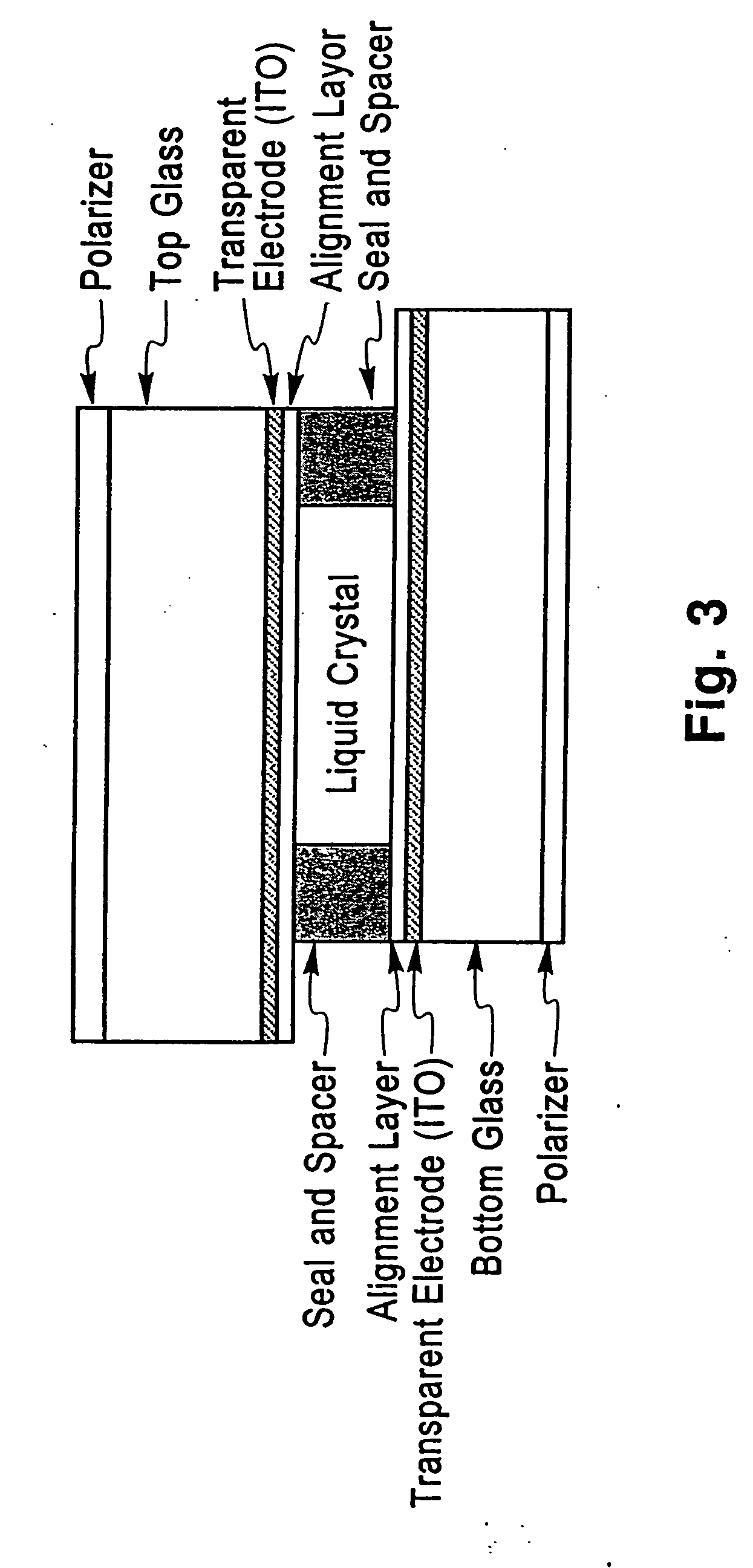
Electronic devices having patterned electrically conductive polymers providing electrical connection thereto and methods of fabrication thereof are described. Liquid crystal display cells are described having at least one of the electrodes providing a bias across the liquid crystal material formed from a patterned electrically conductive polymer. Thin film transistors having patterned electrically conductive polymers as source drain and gate electrodes are described. Light emitting diodes having anode and coated regions formed from patterned electrically conductive polymers are described. Methods of patterning using a resist mask; patterning using a patterned metal layer, patterning the metal layer using a resist; and patterning the electrically conductive polymer directly to form electrodes and anode and cathode regions are described.

Description

[0001] This application claims priority from, and is a continuation-in-part of, International Application No. PCT / US97 / 20862 filed on Nov. 10, 1997 and published on May 22, 1998, the teaching of which is incorporated herein by reference. [0002] This application is a continuation-in-part of copending U.S. application Ser. No. 08 / 476,141 filed Jun. 7, 1995 entitled, “Electrically Conductive and Abrasion / Scratch Resistance Polymeric Materials and Uses Thereof” to Angelopoulos et al., the teaching of which is incorporated herein by reference. U.S. application Ser. No. 08 / 476,141 is a division of U.S. application Ser. No. 08 / 193,926 now issued as U.S. Pat. No. 5,721,299 which is a continuation-in-part of and incorporated by reference U.S. application Ser. No. 08 / 357,565 filed May 26, 1989 issued as U.S. Pat. No. 5,198,153. Thus, the teaching of U.S. application Ser. No. 08 / 357,565 filed May 26, 1989 is incorporated herein by reference. U.S. application Ser. Nos. 08 / 476,141 and 08 / 357,565...

Claims


Application Information

Patent Timeline
Patent Type & Authority Applications(United States)
IPC IPC(8): G02F1/1343C08G61/12C12Q1/68H01B1/12H01J29/86H01L21/033H01L21/311H01L23/498H01L23/60H01L29/45H01L29/49H01L33/38H01L33/40H01L33/42H01L51/05H01L51/40H01L51/52H01S5/042H05K9/00
CPCC08G61/12Y10T428/24331H01B1/125H01B1/127H01B1/128H01J29/868H01L21/0332H01L21/31138H01L23/49894H01L23/60H01L29/456H01L29/458H01L29/4908H01L33/38H01L33/42H01L51/0018H01L51/0021H01L51/0023H01L51/0504H01L51/0508H01L51/0512H01L51/0545H01L51/102H01L51/5203H01L51/5206H01L51/5234H01L2251/5323H01L2924/09701H01L2924/12044Y10T428/1055Y10T428/10Y10T428/12528H01L2924/0002G02F1/13439Y10T428/31692Y10T428/31678Y10T428/31533Y10T428/31504H01L2924/00C09K2323/04C09K2323/00H10K71/233H10K71/621H10K71/60H10K10/46H10K10/462H10K10/466H10K50/81H10K50/828H10K2102/3031H10K50/805H10K10/00H10K10/82
Inventor ANGELOPOULOS, MARIEDIMITRAKOPOULOS, CHRISTOS DIMITRIOSFURMAN, BRUCE KENNETHGRAHAM, TERESITA ORDONEZLIEN, SHUI-CHIH ALAN
Owner GLOBALFOUNDRIES INC
Learn More