Laser Modification and Functionalization of Substrates
a substrate and laser technology, applied in the field of laser modification and functionalization of substrates, to achieve the effects of reducing the cost per slide, and improving the signal-to-noise ratio
- Summary
- Abstract
- Description
- Claims
- Application Information
AI Technical Summary
Benefits of technology
Problems solved by technology
Method used
Image
Examples
example 1
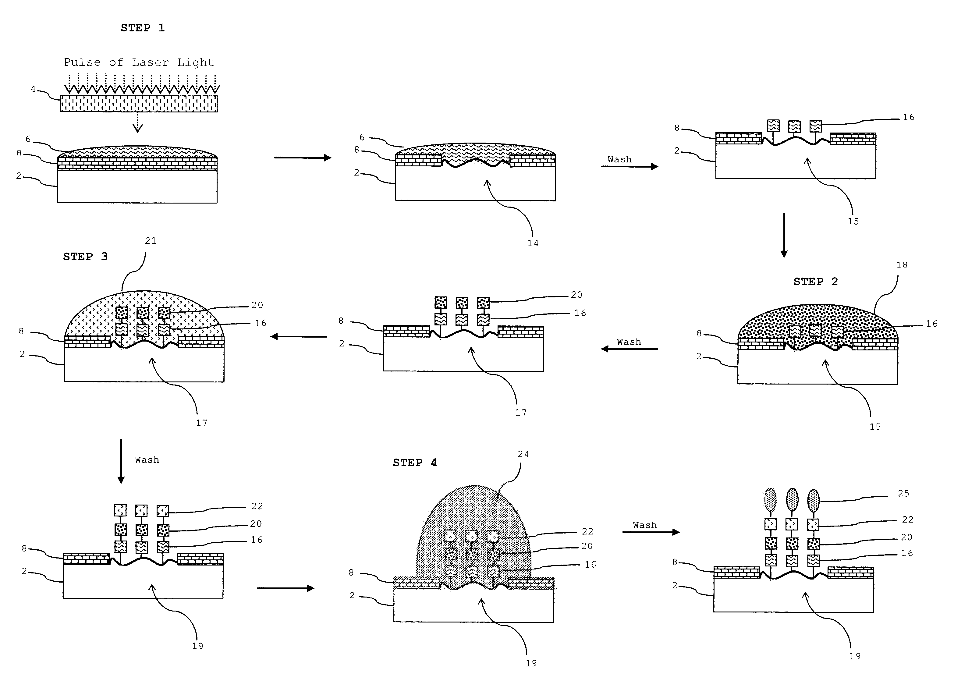
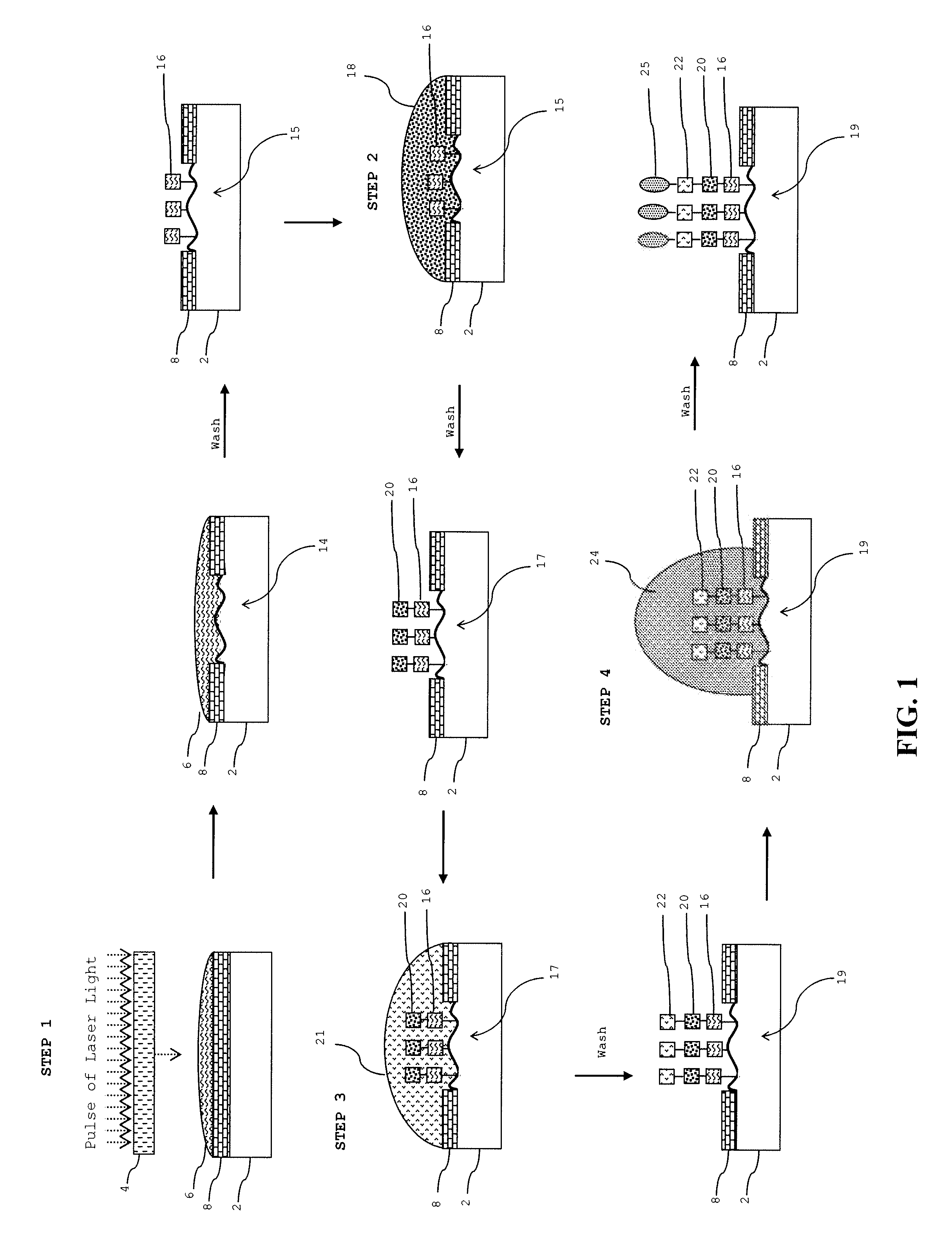
[0086] In this example we show that we can wet a semiconductor surface, e.g., silicon or germanium, with a reactive compound and then fire a highly focused, nanosecond pulse of laser light through the transparent liquid onto the surface. The high peak power of the pulse at the surface activates the surface so that it reacts with the liquid it is in contact with. This work was performed with single lenses, not microlens arrays. Similar and sometimes identical chemistry occurs using microlens arrays. Unless otherwise indicated experimental conditions for the results in this example are as follows: 532 nm light from a Coherent Infinity Nd:YAG laser, with a 4 ns pulse width, 50-100 μJ pulse energy, and the calculated diameter of the laser at the surface is 50-100 μm. Average values and errors (standard deviations) in this work are from three measurements.
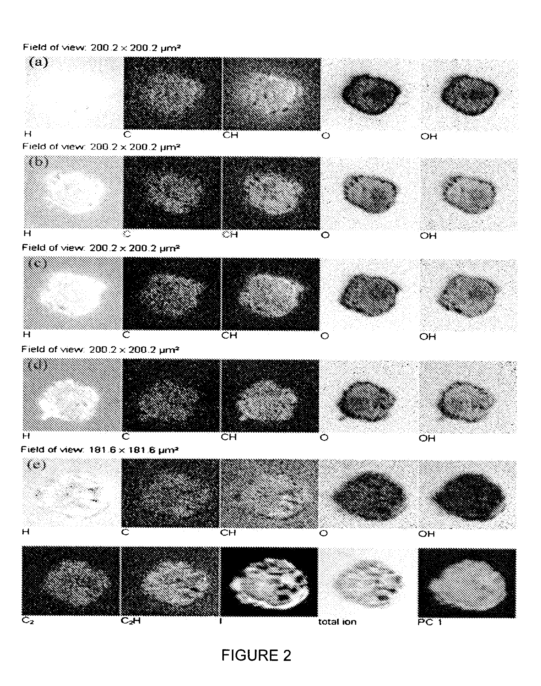
[0087]FIG. 2 shows representative time-of-flight secondary ion mass spectrometry (ToF-SIMS, ION-TOF IV) negative ion images of spots ...
example 2
[0095] Sample Cleaning. Pieces of silicon were cleaned with a 2% solution of sodium dodecyl sulfate (a surfactant). They were then plasma cleaned in a Harrick plasma cleaner (5 minutes on high power).
[0096] Hydrophobic Monolayer Formation: After this second cleaning, the surfaces were put in a 5% aqueous solution of HF for 8 minutes to remove the native oxide layer on the silicon surface and leave behind hydrogen-terminated silicon. This hydrogen-terminated silicon was then immersed in neat (pure) 1-hexadecene (≧99.0), which had been degassed by bubbling nitrogen gas through it for an hour. After the silicon was put in the 1-hexadecene the liquid was further degassed by bubbling with nitrogen for at least another 0.5 hr. The pure 1-hexadecene with the silicon shard in it was then heated to 210° C. for 1 hour.
[0097] Sample Cleaning: The silicon samples were then removed and washed several times with hexane and ethanol. The surfaces were further cleaned by sonication twice in methyl...
PUM
| Property | Measurement | Unit |
|---|---|---|
| sizes | aaaaa | aaaaa |
| thickness | aaaaa | aaaaa |
| thickness | aaaaa | aaaaa |
Abstract
Description
Claims
Application Information
 - R&D
- Intellectual Property
- Life Sciences
- Materials
- Tech Scout
- Unparalleled Data Quality
- Higher Quality Content
- 60% Fewer Hallucinations
Browse by: Latest US Patents, China's latest patents, Technical Efficacy Thesaurus, Application Domain, Technology Topic, Popular Technical Reports.
© 2025 PatSnap. All rights reserved.Legal|Privacy policy|Modern Slavery Act Transparency Statement|Sitemap|About US| Contact US: help@patsnap.com


