Photoconductive imaging member
- Summary
- Abstract
- Description
- Claims
- Application Information
AI Technical Summary
Benefits of technology
Problems solved by technology
Method used
Image
Examples
example 1
Preparation of Photogenerating Layer of Imaging Member
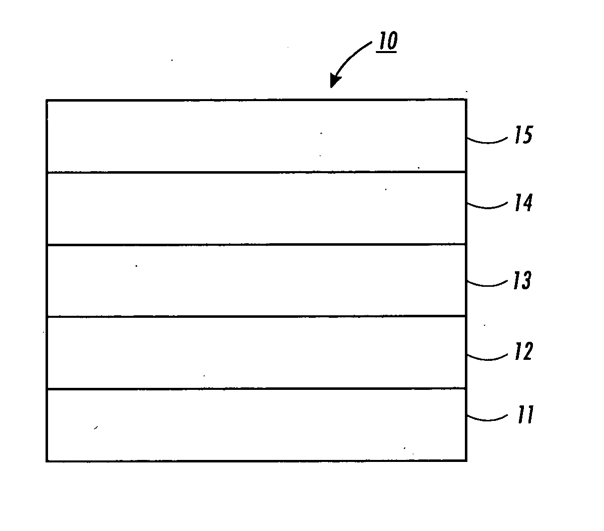
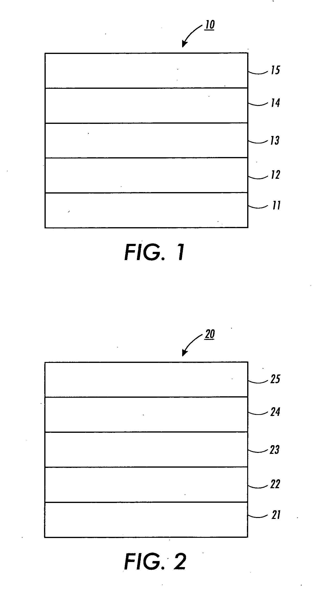
[0068] An imaging member was prepared by providing a 0.02 micrometer thick titanium layer coated on a biaxially oriented polyethylene naphthalate substrate (KALEDEX™ 2000) having a thickness of 3.5 mils. Applied thereon with a gravure applicator, was a solution containing 50 grams 3-amino-propyltriethoxysilane, 41.2 grams water, 15 grams acetic acid, 684.8 grams of 200 proof denatured alcohol and 200 grams heptane. This layer was then dried for about 5 minutes at 135° C. in the forced air drier of the coater. The resulting blocking layer had a dry thickness of 500 Angstroms.
[0069] An adhesive layer was then prepared by applying a wet coating over the blocking layer, using a gravure applicator, containing 0.2 percent by weight based on the total weight of the solution of polyarylate adhesive (Ardel D100 available from Toyota Hsutsu Inc.) in a 60:30:10 volume ratio mixture of tetrahydrofuran / monochlorobenzene / methylene chloride. ...
example 2
[0071] Coating with Transport Layer
[0072] A coating sample of Example I was coated with a transport layer containing 50 weight percent (based on the total solids) of hole transport compound, N,N′-diphenyl-N,N′-bis(3-methyl-phenyl)-(1,1′-biphenyl)-4,4′-diamine.
[0073] In a four ounce brown bottle, 10 grams of MAKROLON® 5705 (available from Bayer Chemicals) was dissolved in 113 grams of methylene chloride. After the polymer was completely dissolved, 10 grams of N,N′-diphenyl-N,N′-bis(3-methylphenyl)-1,1′-biphenyl-4˜4′-diamine was added to the solution. The mixture was shaken overnight to assure a complete solution. The solution was applied onto the photogenerating layer made in Example 1 using a 4.5 mil Bird bar to form a coating. The coated device was then heated in a forced air oven at 120° C. for 1 minute to form a charge transport layer having a dry thickness of 29 micrometers.
example 3
[0074] A photoreceptor was prepared as in example 2 except for the following. The transport layer solution was prepared by using an amount of 9.9 gm MAKROLON® 5705, and 0.1 gm of Ardel D-100 polyarylate. The mixture has 0.5% polyarylate based on overall solids.
PUM
 Abstract
Description
Claims
Application Information
 - R&D Engineer
- R&D Manager
- IP Professional
- Industry Leading Data Capabilities
- Powerful AI technology
- Patent DNA Extraction
Browse by: Latest US Patents, China's latest patents, Technical Efficacy Thesaurus, Application Domain, Technology Topic, Popular Technical Reports.
© 2024 PatSnap. All rights reserved.Legal|Privacy policy|Modern Slavery Act Transparency Statement|Sitemap|About US| Contact US: help@patsnap.com


