
Laminated ceramic electronic component

a technology of laminated ceramics and electronic components, applied in the direction of fixed capacitor details, gymnastic exercise, fixed capacitors, etc., can solve the problems of affecting the manufacturing process, affecting the quality of the product, and causing cracks, etc., to inhibit the occurrence of separation, delamination and cracks

Active Publication Date: 2006-09-28
TDK CORPARATION
View PDF6 Cites 34 Cited by
  • Summary
  • Abstract
  • Description
  • Claims
  • Application Information

AI Technical Summary

Benefits of technology

[0011] It is another object of the present invention to provide a laminated ceramic electronic component which is excellent in electrical characteristics.
[0024] As has been described hereinabove, the present invention has at least one of the following advantages: (a) Providing a laminated ceramic electronic component which is capable of inhibiting occurrence of separation, delamination and cracks. (b) Providing a laminated ceramic electronic component which is excellent in electrical characteristics. (c) Providing a laminated ceramic electronic component which is capable of enhancing production yield. (d) Providing a laminated ceramic electronic component which is easy to manufacture.

Problems solved by technology

The difference in burning shrinkage / thermal expansion coefficient between the functional layer and the protective layer produces a large stress along an interface between them during the process of manufacturing the laminate ceramic electronic components, which tends to cause separation, delamination and cracks.
Particularly, there is a problem that cracks tend to be caused by heat treatment (or annealing) or burning with stress remaining therein.
However, the technology disclosed in JP 2003-309039 has a problem of complicating the manufacturing process because of the necessity of a plurality of sheets with different binder contents.
In addition, since the stress and physical strain along the interface between the functional layer and the protective layer increase with thinning and multi-layering, the above-mentioned problems are becoming more prominent due to thinning, multi-layering, and greater density of recent laminated ceramic electronic components.

Method used


Image

  • Laminated ceramic electronic component
  • Laminated ceramic electronic component
  • Laminated ceramic electronic component

Examples


Embodiment Construction

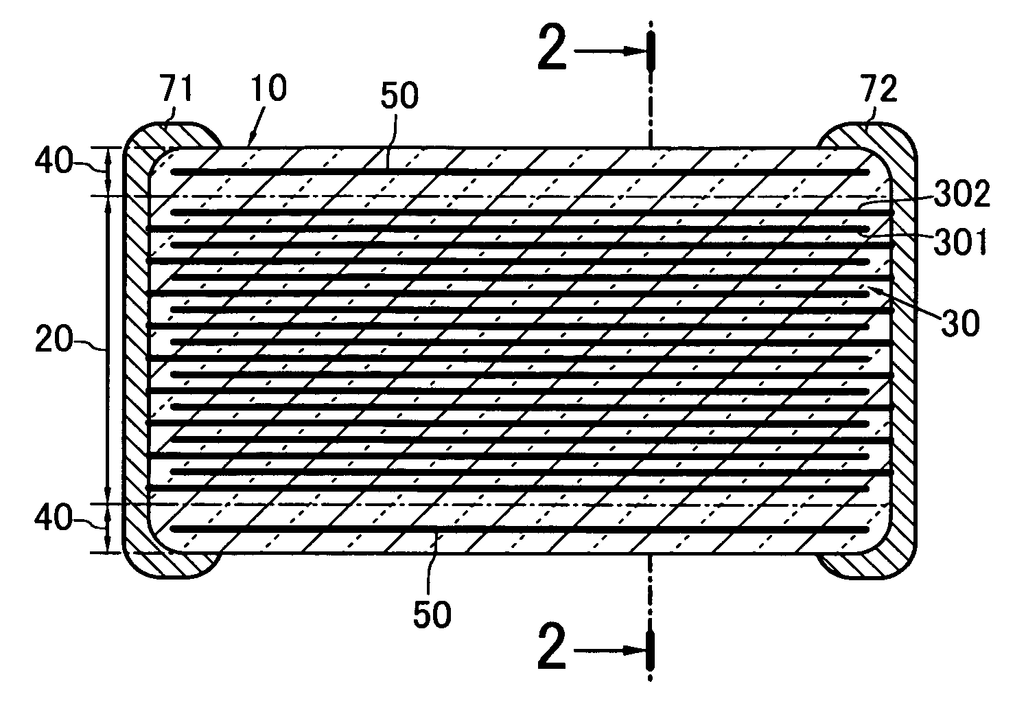
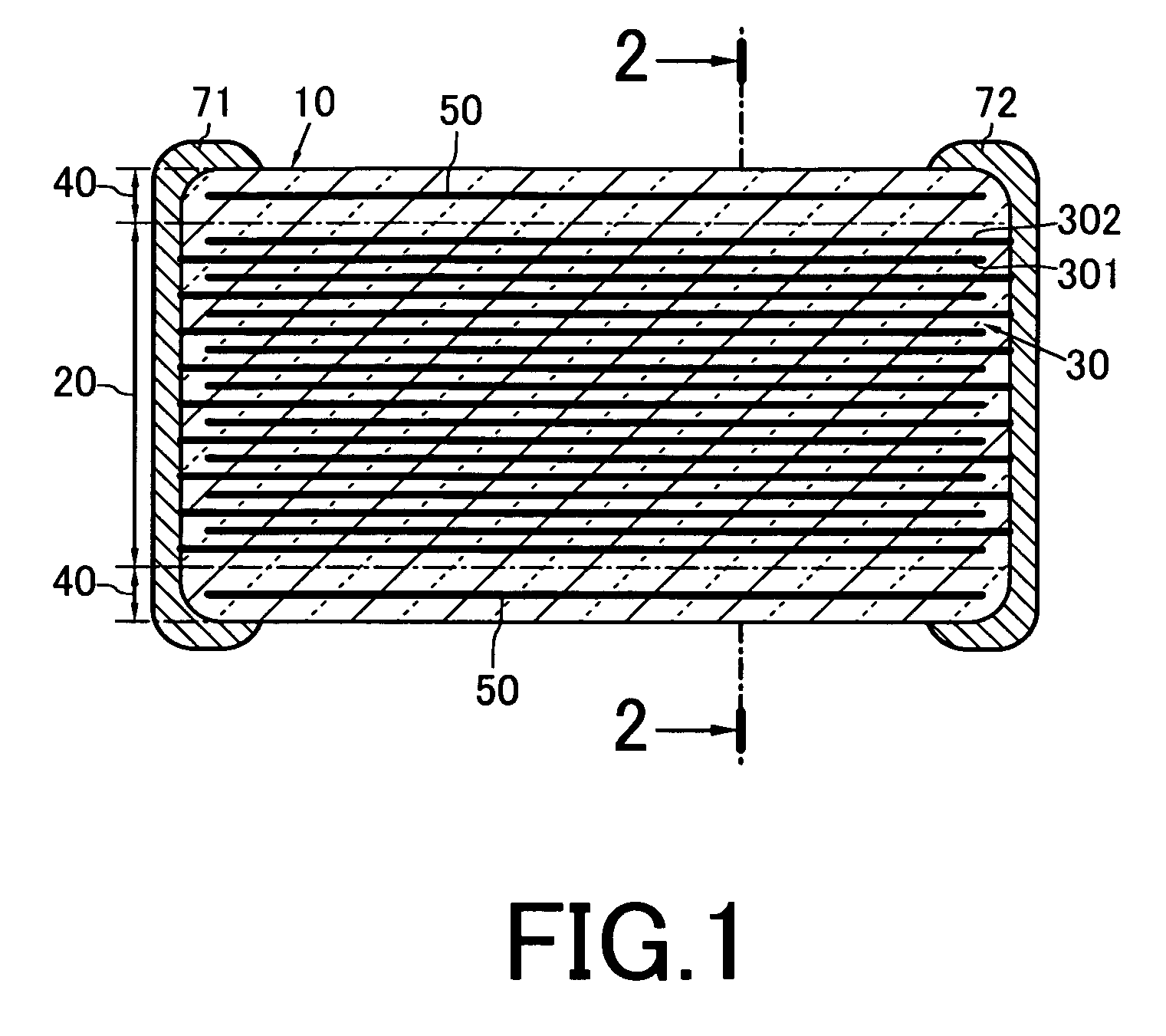
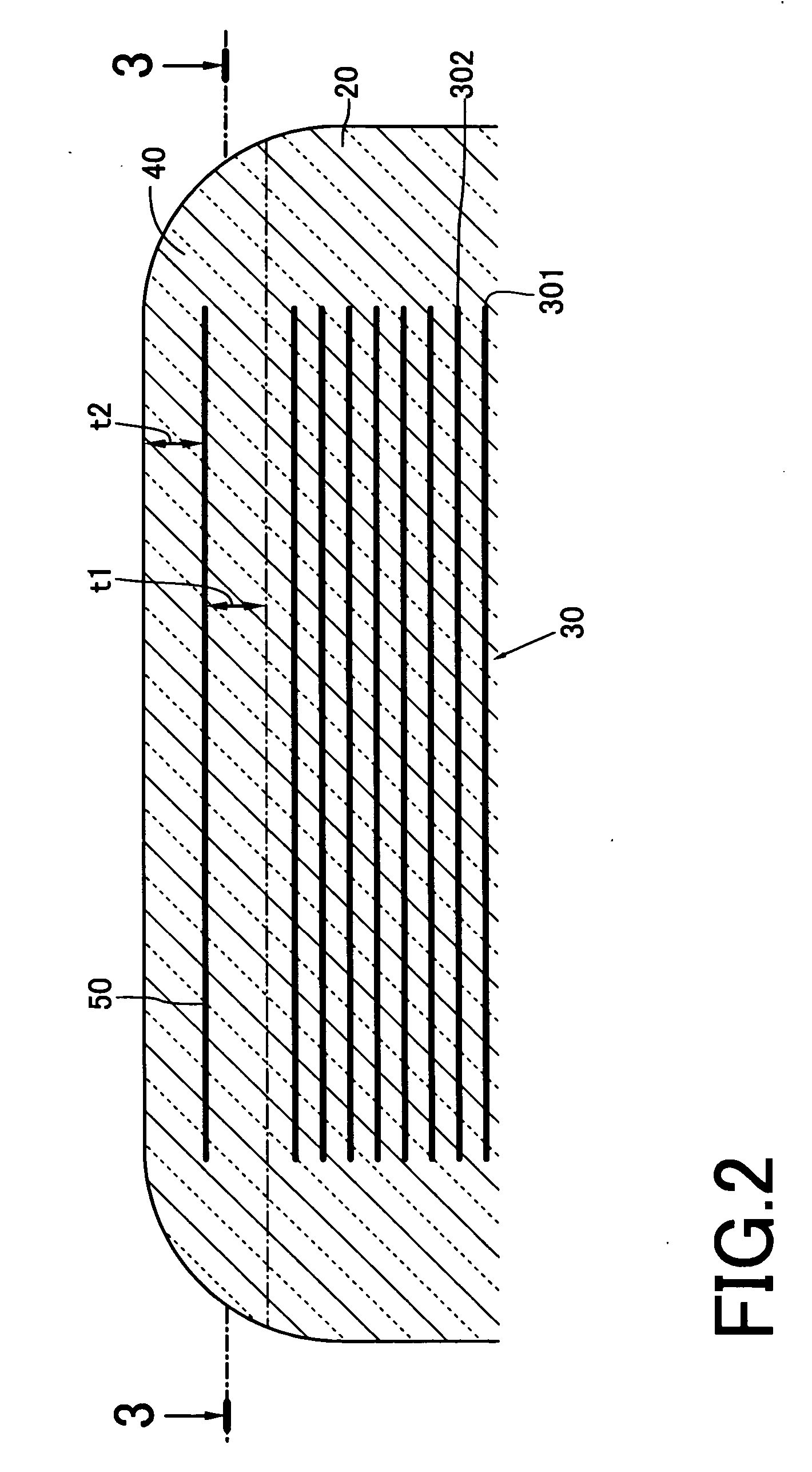
[0038] Referring to FIGS. 1 to 3, a laminated ceramic electronic component includes a ceramic substrate 10, an internal electrode 30, and buffer layers 50. The ceramic substrate 10 includes a functional layer 20 and protective layers 40. The illustrated laminated ceramic electronic component may be adopted as a laminated ceramic capacitor, a laminated ceramic inductor, a multilayer ceramic substrate and the like.

[0039] The protective layer 40 is provided to protect the functional layer 20. In FIG. 1, both the top and bottom sides of the functional layer 20 are covered with the protective layers 40, but it is also possible to provide only one protective layer 40 on either of the top and bottom sides of the functional layer 20.

[0040] The ceramic substrate constituting the functional layer 20 and the ceramic substrate constituting the protective layer 40 may have the same composition or different compositions. For example, the functional layer 20 and the protective layer 40 may be ma...


PUM


Abstract

A laminated ceramic electronic component includes a ceramic substrate, an internal electrode, and a buffer layer. The ceramic substrate includes a protective layer and a functional layer. The protective layer is disposed on at least one side of the functional layer. The internal electrode is embedded in the functional layer. The buffer layer is embedded in the protective layer and has a different burning shrinkage from the ceramic substrate.

Description

BACKGROUND OF THE INVENTION [0001] 1. Field of the Invention [0002] The present invention relates to a laminated ceramic electronic component. [0003] 2. Description of the Related Art [0004] Electronic devices with laminated ceramic electronic components such as a laminated ceramic capacitor and a laminated ceramic substrate are becoming smaller in size with an attempt to achieve higher performance and greater functionality. In order to keep up with the technology trends, it is also required to improve characteristics and achieve downsizing of the laminated ceramic electronic components by further thinning, multi-layering, and greater density. [0005] The laminated ceramic electronic components generally include a functional layer embedded with an internal electrode and protective layers disposed on both sides of the functional layer. Typically, since no internal electrode is embedded in the protective layer, the protective layer differs from the functional layer in burning shrinkage...

Claims


Application Information

Patent Timeline
IPC IPC(8): H01G4/06
CPCH01G4/30A63B5/20A63B21/023A63B21/055
Inventor TONOGAI, TORUKOJIMA, TATSUYAIWASAKI, AKINORIMASAOKA, RAITAROMUROSAWA, SHOGOYAMAGUCHI, AKIRAABE, KYOTAROSATO, TSUKASA
Owner TDK CORPARATION
Learn More