
Static random access memory utilizing gated diode technology

a gated diode and memory technology, applied in static storage, information storage, digital storage, etc., can solve the problems of degrading the stability of the sram cell, insufficient low level charge, etc., and achieve high signal to noise ratio, high signal margin, and high performance.

Active Publication Date: 2006-09-07
GLOBALFOUNDRIES US INC
View PDF4 Cites 29 Cited by
  • Summary
  • Abstract
  • Description
  • Claims
  • Application Information

AI Technical Summary

Benefits of technology

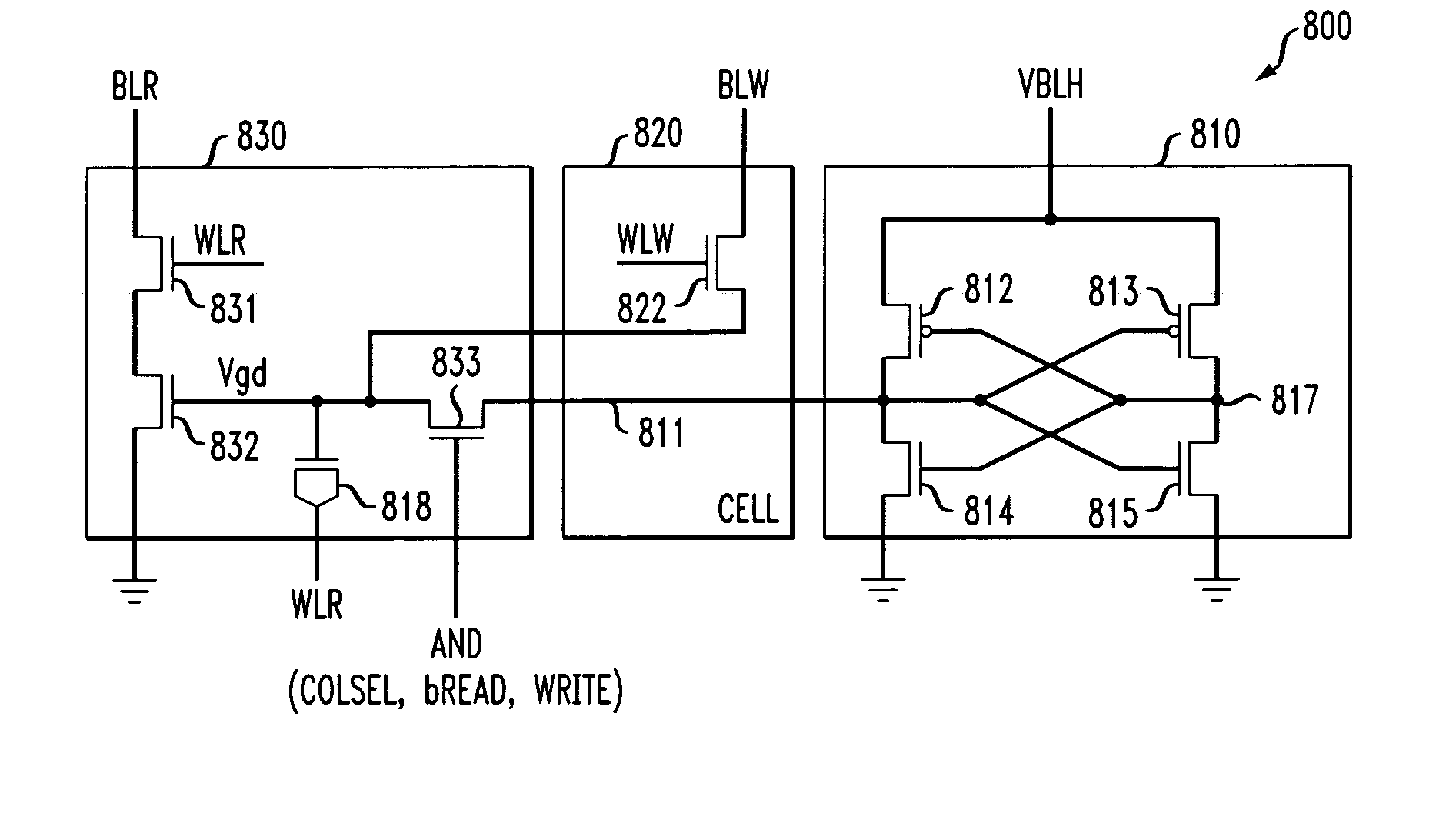
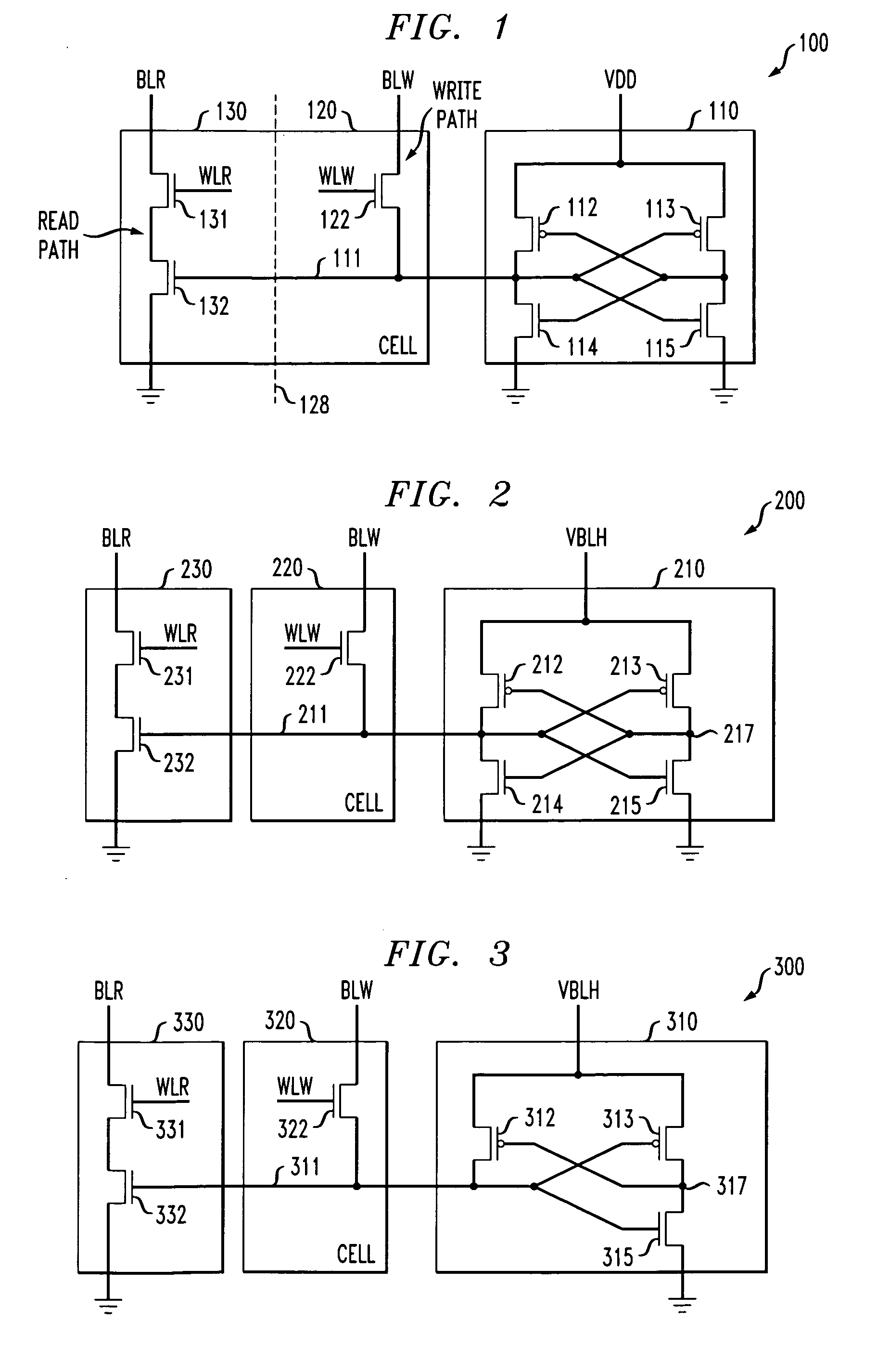
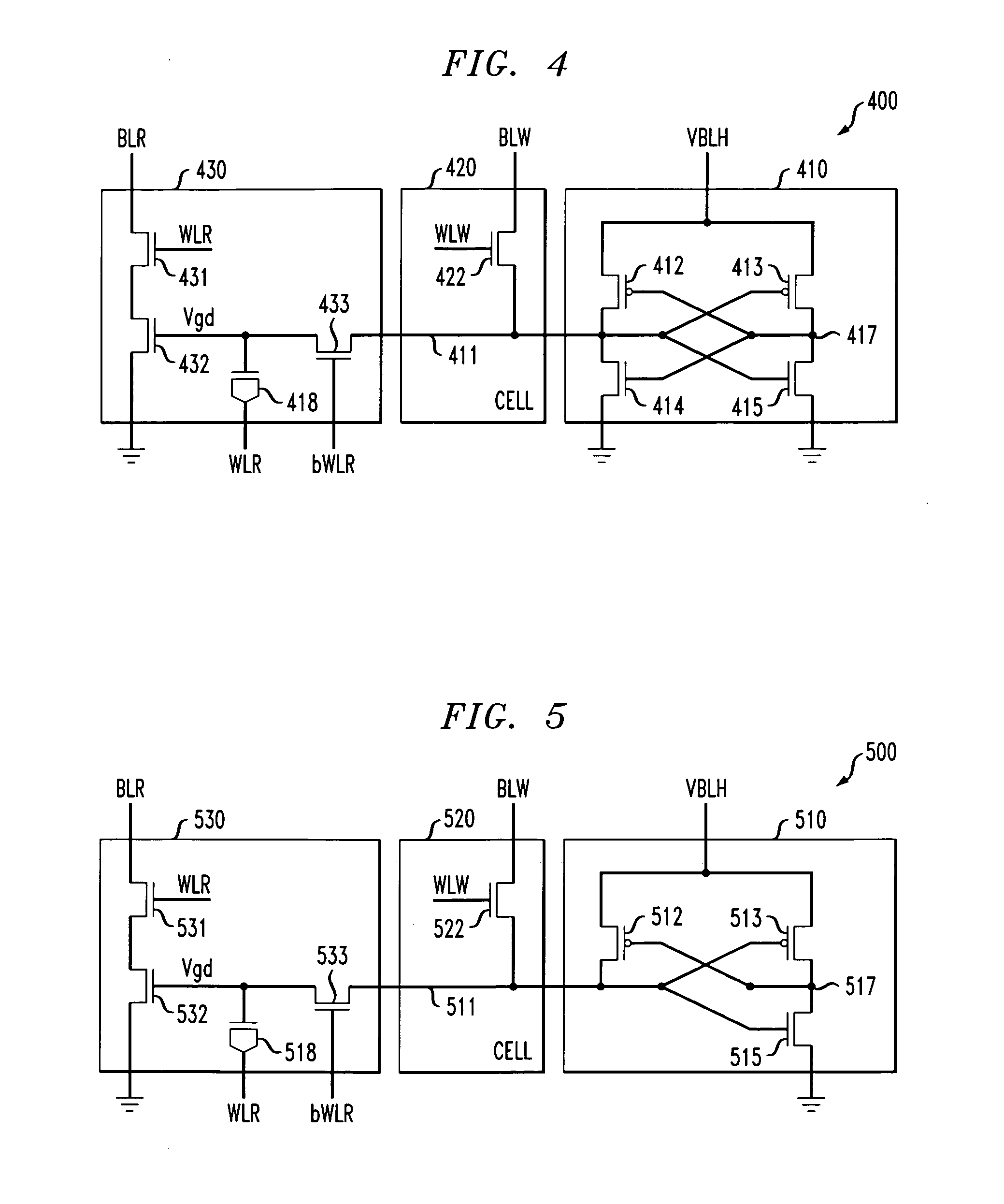
[0007] A new type of static RAM cell is disclosed that is based on a gated diode and its voltage amplification characteristic. The cell combines the advantages of a static RAM, in which data refresh is not needed, and those of gated diode cells, which are scalable to low voltages, have a high signal to noise ratio, high signal margin, and tolerance to process variations, to form a single high performance static memory cell. This new cell has independent read and write paths, which allow for separate optimization of the two read / write (R / W) events and enable dual-port R / W operation. Furthermore, storage node disturbs during the read operation are eliminated, which greatly improves cell stability and scalability for future technologies.
[0008] A static gain cell is formed by combining a 4-transistor (4T) static latch and a 3-transistor (3T) gain cell with single-ended R / W ports (a total of 7 transistors). An alternative embodiment with only 6 transistors is also disclosed. The addition of a gated diode to the static gain cell, forming a static gated diode RAM cell, allows for amplification of the internal cell voltage during the read operation, which allows for the use of a very low supply voltage in the memory array while still achieving high performance, in terms of both read and write speed. The gated diode structure can be very simple as there are only loose restrictions on its electrical parameters (e.g., threshold voltage). A number of embodiments of the static gated diode RAM cell, with different circuit configurations and transistor counts, are disclosed, including a basic, minimal cell consisting of six transistors and a gated diode with separate read / write ports to a cell with eight transistors and a gated diode.

Problems solved by technology

The low level charge is insufficient to maintain storage of the data.
With the growing influence of process-induced variations, threshold voltage fluctuations further degrade the SRAM cell stability.

Method used


Image

  • Static random access memory utilizing gated diode technology
  • Static random access memory utilizing gated diode technology
  • Static random access memory utilizing gated diode technology

Examples


Embodiment Construction

[0027] A number of static random access memory (static RAM or SRAM) cells based on a gated diode are disclosed. Each static gated diode random access memory cell is comprised of a static storage element, such as a static latch, for holding the 0- and 1-data indefinitely (for as long as the power is ON), and a gated diode circuit for storing and amplifying the cell voltage during a read operation. The memory cells can perform a non-destructive read operation, do not require refresh, and can potentially become a replacement for conventional SRAM, such as 6T SRAM.

[0028] The read and write paths of the memory cell are single-ended and are independent of each other. As a result, the read and write operations can be individually optimized for speed and power. The memory cell can be structured as single- or dual-port, which can allow for concurrent read and write operations for cells in the same array with different addresses.

[0029] Due to the voltage amplification of the cell voltage by...


PUM


Abstract

A new type of static RAM cell is disclosed that is based on a gated diode and its voltage amplification characteristic. The cell combines the advantages of a static RAM, in which data refresh is not needed, and those of gated diode cells, which are scalable to low voltages, have high signal to noise ratio, high signal margin, and tolerance to process variations, to form a single high performance static memory cell. This new cell has independent read and write paths, which allow for separate optimization of the read (R) and write (W) events, and enable dual-port R / W operation. Furthermore, storage node disturbance during the read and write operations are eliminated, which greatly improves cell stability and scalability for future technologies.

Description

FIELD OF THE INVENTION [0001] The present invention relates to memory circuits and, more particularly, to memory circuits that utilize gated diode circuits. BACKGROUND OF THE INVENTION [0002] The small signal amplification characteristics of the gated diode device structure were originally used to create signal amplifiers and dynamic memory cells, including one transistor one diode (1T1D), two transistor one diode (2T1D), and three transistor one diode (3T1D) memory cells. U.S. patent application Ser. No. 10 / 735,061, entitled “Gated Diode Memory Cells,” incorporated by reference herein, describes 1T1D and 2T1D gated diode memory cells, a new type of dynamic memory cell with internal voltage amplification based on gated diode circuits and structures. U.S. patent application Ser. No. 10 / 751,714, entitled “Amplifiers Using Gated Diodes,” incorporated by reference herein, describes gated diode circuits for signal amplification that are suitable for amplifying small amplitude signals. U....

Claims


Application Information

Patent Timeline
IPC IPC(8): G11C11/00
CPCG11C11/413
Inventor LUK, WING KINCHANG, LELAND
Owner GLOBALFOUNDRIES US INC
Learn More