Voltage-controlled oscillator

Inactive Publication Date: 2006-07-27
COLLABO INNOVATIONS INC
View PDF4 Cites 9 Cited by
  • Summary
  • Abstract
  • Description
  • Claims
  • Application Information

AI Technical Summary

Benefits of technology

[0018] This invention is made in consideration of the above mentioned problems and it is an advantage of the invention that the invention provides a voltage-controlled oscillator which does not reduce a variable range of frequency and is easy to control oscillation frequency.
[0019] That is, it is another advantage of the invention that the invention provides a voltage-controlled oscillator which reduces a deviation of static capacitance to equal to or more than a capacitance switching voltage or equal to or less than the capacitance switching voltage by preventing the static capacitance generated between terminals of the MOS transistor from increasing equal to or less than the capacitance switching voltage, and is capable of controlling a threshold voltage of the MOS transistor independently of a temperature characteristic compensation signal and an external voltage frequency control signal.
[0020] In order to achieve the above-mentioned advantage, a voltage-controlled oscillator according to the invention includes: an amplifier which includes an inverter and a feedback resistor; a piezoelectric vibrator which is connected to input and output terminals of the amplifier; a variable capacitive element which includes a variable capacitor and first and second DC cut capacitors in which each one end thereof is respectively connected to both terminals of the piezoelectric vibrator severing as a load capacitance between the terminals of the piezoelectric vibrator. The variable capacitor includes: first and second MOS transistors, in which a drain terminal is connected to the other end of the first and second DC cut capacitors, source and backgate terminals are shorted to each other, and a gate terminal is shorted; first and second high-frequency elimination resistors in which one end thereof is connected to each of a source-backgate terminal of the first and second MOS transistors; and third and fourth high-frequency elimination resistors in which one end thereof is respectively connected to each of the drain terminals of the first and second MOS transistors and the other end is connected to each other. The voltage-controlled oscillator includes a static capacitance generated between the drain and gate terminals of the first MOS transistor and a static capacitance generated between the drain and gate terminals of the second MOS transistor. The voltage-controlled oscillator controls an oscillation frequency by using a first control signal which is input to the gate terminals connected to the first and second MOS transistors when an oscillation voltage is applied to the drain terminals of the first and second MOS transistors, and a second control signal which is input to each drain terminals of the first and second MOS transistors through the third and fourth high-frequency elimination resistors, respectively, and is input to the source-backgate terminals of the first and second MOS transistors through the first and second high-frequency elimination resistors, respectively.
[0021] According to the above-mentioned configuration, it is possible to minimize a capacitance and to increase the variable amount of frequency equal to or less than the capacitance switching voltage by changing a connection of the first and second MOS transistors and adding the first to fourth high-frequency elimination resistors and the first and second DC cut capacitors without increasing the number of elements, thus reducing the device size. In addition, it is possible to control the threshold voltage of the MOS transistor to control the capacitance switching voltage by using first and second control signals which can be independently controlled, and to change the frequency based on a predetermined control voltage. Further, it is possible to reduce the deviation of capacitance equal to, more or less than capacitance switching voltage, thereby reducing the deviation of oscillation frequency of the voltage-controlled oscillator.
[0022] In addition, it is preferable that the MOS transistors capable of controlling the capacitance switching voltage is connected to both terminals of the piezoelectric vibrator. However, it is also preferable that the MOS transistor capable of controlling the capacitance switching voltage is connected to only one end of the piezoelectric vibrator so as to input a control signal to the other end through the high-frequency elimination resistor.
[0023] That is, a voltage-controlled oscillator according to the invention includes: an amplifier which includes an inverter and a feedback resistor; a piezoelectric vibrator which is connected to input and output terminals of the amplifier; a variable capacitive element which includes a variable capacitor and first and second DC cut capacitors which are disposed between both terminals of the piezoelectric vibrator and each of which is connected to one end of the piezoelectric vibrator, and a variable capacitor, in which the variable capacitor includes: a MOS transistor having a drain terminal connected to the other end of the first or second DC cut capacitor, source and backgate terminals shorted to each other, and a gate terminal shorted to a gate terminal of the remaining MOS transistor; a first high-frequency elimination resistor connected to one end of the source-backgate terminal of the MOS transistor; and a third high-frequency elimination resistor connected to one end of the drain terminal of the MOS transistor, and in which the voltage-controlled oscillator controls an oscillation frequency by varying a static capacitance generated between the drain and gate terminals of the MOS transistor by means of a first control signal which is input to the gate terminal of the MOS transistor when an oscillation voltage is applied to the drain terminal of the MOS transistor, and a second control signal which is input to the other end of the first or second DC cut capacitor through the fourth high-frequency elimination resistor.

Problems solved by technology

As a first problem of the above-mentioned voltage-controlled oscillator according to the related art, since DC bias of a drain terminal is determined on an amplifier side of an oscillation circuit, it is not possible to set a capacitance switching voltage to a predetermined value and it is thus not possible to control a frequency based on a predetermined gate voltage.
As a second problem that in a typical CMOS process, the capacitance switching voltage is changed depending on a deviation in threshold voltage or the temperature characteristic of a MOS transistor.
Thus, there is another problem in that a deviation of the oscillation frequency characteristic of the voltage-controlled oscillator in the example according to the related art with respect to a voltage between the gate terminal and the source-drain terminal is large as shown in FIG. 19B, such that the characteristic of the control voltage becomes complicated.
As a third problem, there is another problem in that since the capacitance value is large when the gate voltage is less than the capacitance switching voltage, a variable range of a frequency is small.
As a fourth problem, due to a deviation between an impurity concentration of a channel of a MOS transistor and a concentration of an N-type semiconductor area, a parasitic capacitance between the source-drain terminal and the ground terminal of a MOS variable capacitor is dispersed and a load capacitor of an oscillator is dispersed, thereby increasing a deviation of oscillation frequency.
Accordingly, in order to facilitate designing a crystal oscillator using the static capacitance generated between the source-drain terminal and the gate terminal, there is a problem in that the static capacitance generated between terminals of the MOS transistor is required to be enlarged or the static capacitance is required to be enlarged through the use of an array structure, the threshold voltage control signal of the MOS transistor needs to be controlled independently of the temperature characteristic compensation signal and the external voltage frequency control signal, and the deviation of static capacitance generated between the source-drain terminal and the gate terminal needs to be reduced.

Method used


Image

  • Voltage-controlled oscillator
  • Voltage-controlled oscillator
  • Voltage-controlled oscillator

Examples


first embodiment

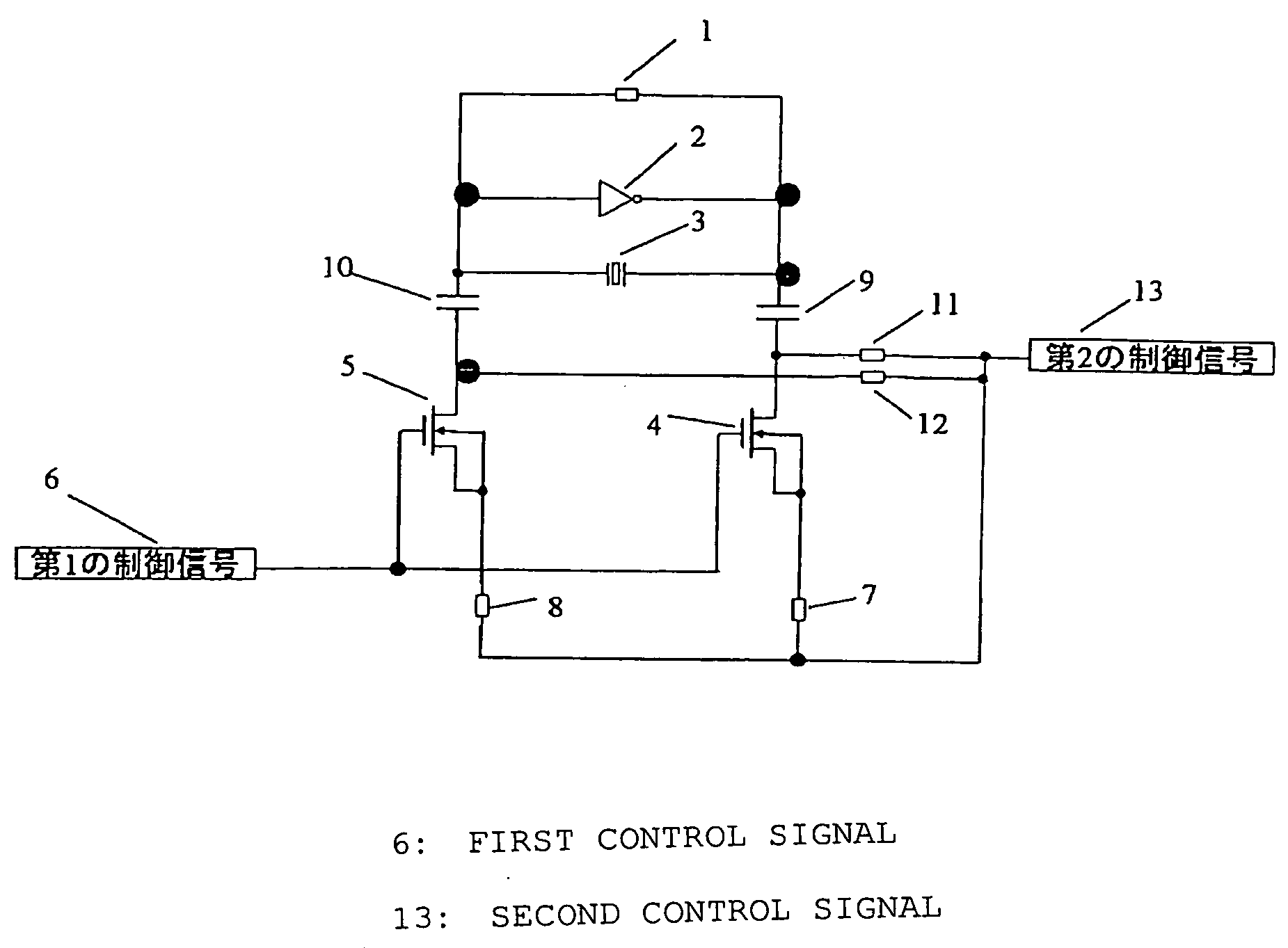
[0073]FIG. 1 is a circuit diagram showing a configuration of a voltage-controlled oscillator according to a first embodiment of the invention.

[0074] The voltage-controlled oscillator according to the this embodiment includes an amplifier, which has a feedback resistor 1 and an inverter 2, a piezoelectric vibrator 3, which is connected to input and output terminals of the inverter 2, first and second DC cut capacitors 9 and 10, in which each one end thereof is connected to both terminals of the piezoelectric vibrator 3 is connected to one end of the piezoelectric vibrator 3, a load capacitor having first and second MOS transistors 4 and 5, in which each drain terminal is connected to the other end of each of the first and second DC cut capacitors 9 and 10, source and backgate terminals are shorted to each other, and each gate terminal is shorted from the other gate terminal, first and second high-frequency elimination resistors 7 and 8, in which each one end thereof is connected to ...

second embodiment

[0090]FIG. 5 is a circuit diagram showing a configuration of a voltage-controlled oscillator according to a second embodiment of the invention.

[0091] The voltage-controlled oscillator according to the second embodiment is configured such that the first DC cut capacitor 9 and the second DC cut capacitor 10 are connected between both terminals of the inverter 2 and both terminals of the piezoelectric vibrator 3 in the voltage-controlled oscillator according to the first embodiment.

[0092] According to the above-mentioned configuration, the voltage-controlled oscillator according to the second embodiment has the same feature as that of the voltage-controlled oscillator according to the first embodiment. In addition, since the MOS variable capacitor consisting of the first and second MOS transistors 4 and 5 and the first and second DC cut capacitors 9 and 10 are connected in parallel to each other when viewed from the piezoelectric vibrator 3, it is possible to increase an absolute val...

third embodiment

[0093]FIG. 6 is a circuit diagram showing a configuration of a voltage-controlled oscillator according to a third embodiment of the invention.

[0094] A voltage-controlled oscillator according to the third embodiment is configured such that the first control signal 6 is supplied from the first control signal generation circuit 6a, and the second control signal 13 is supplied from the second control signal generation circuit 13a in the voltage-controlled oscillator according to the first embodiment.

[0095] According to the above-mentioned configuration, the voltage-controlled oscillator according to the third embodiment has the same feature as that of the voltage-controlled oscillator according to the first embodiment. In addition, the first and second control signals 6 and 13 can be supplied from a circuit integrated with the voltage-controlled oscillator rather than an external device, thereby reducing the size of a system that uses the voltage-controlled oscillator.


PUM


Abstract

With a variable capacitor including a load capacitor of an oscillation circuit having a feedback resistor 1, an inverter 2, and a crystal oscillator 3, and a static capacitance generated between a drain terminal and a gate terminal of MOS transistors 4 and 5, in which source and backgate terminals are shorted to each other, a serial connection of a DC cut capacitor 9, 10 and a variable capacitors (MOS transistor) 4 and 5 is formed between one end and the other end of the crystal oscillator 3. For example, a threshold voltage control signal of the MOS transistors 4 and 5 is input to the drain terminal through a high-frequency elimination resistor 11, 12, and is input to the source-backgate terminal through a high-frequency elimination resistor 7, 8. In addition, a signal obtained by overlapping a temperature characteristic compensation signal and a threshold voltage control signal of the MOS transistor 4, 5 is input to the gate terminal. Accordingly, it is possible to indiscriminately determine an output bias of a temperature compensation control circuit or an external voltage frequency control circuit.

Description

BACKGROUND OF THE INVENTION [0001] 1. Field of the Invention [0002] The present invention relates to a voltage-controlled oscillator and, more particularly, to a voltage-controlled oscillator that is used as a voltage-controlled temperature-compensated crystal oscillator. [0003] 2. Description of the Related Art [0004] In recent years, with rapid development of mobile communication devices, such as mobile phones, the mobile communication devices are required to have a temperature compensation function, to be miniaturized, and to use a higher frequency. Similarly to the mobile communication devices, a crystal oscillator, which has been used in the mobile communication devices as a standard of a communication frequency, is also required to have a temperature compensation function, to be miniaturized, and to use a higher frequency. [0005] A temperature-compensated crystal oscillator has a temperature compensation function and is designed to reduce a variation of frequency due to temper...

Claims


Application Information

Patent Timeline
IPC IPC(8): H03B5/32
CPCH03B5/366H03B2201/0208
Inventor MATSUURA, JUNICHI
Owner COLLABO INNOVATIONS INC
Why Eureka
Try Eureka