Synthesis method for a compound used to form a self-assembled monolayer, compound for forming a self-assembled monolayer, and layer structure for a semiconductor component

a technology of compound and monolayer, applied in the field of semiconductor manufacturing, can solve the problems of high cost of silicon-based chips, inability to use silicon-based identification tags for food marking, and low efficiency of silicon-based chips, and achieve the effect of efficient use for production

Inactive Publication Date: 2006-07-20
QIMONDA
View PDF6 Cites 13 Cited by
  • Summary
  • Abstract
  • Description
  • Claims
  • Application Information

AI Technical Summary

Benefits of technology

[0015] Embodiments of the present invention provide an efficient synthesis method for a compound capable of a π-π interaction with other compounds of the same type and / or compounds of a different type. Furthermore, embodiments provide suitable compounds and a layer structure which may be used efficiently for the production of semiconductor components.
[0018] Owing to the high yield and the possibility of easy purification, economical preparation of suitable compounds is permitted by this two-stage synthesis method.
[0019] Other embodiments of the invention provide compounds for forming self-assembled monolayers, preferably monolayers for semiconductor components. In an embodiment, the compounds are used for a dielectric layer having a stabilizing head group. The head groups interact with one another in order to provide a stable surface of a molecular monolayer which may be easily further structured.

Problems solved by technology

Silicon-based transponders therefore operate at supply voltages of about 3 V. Products which contain a silicon-based chip are too expensive for many applications.
For example, a silicon-based identification tag is not suitable for the marking of foods (price, expiry date, etc.).
To ensure the functionality, the individual layers must be structured, which is relatively complicated.
However, this procedure encounters its limits when it is intended to achieve layer thicknesses of less than 50 nm.
It is disadvantageous that these layers do not form a dense dielectric layer without aftertreatment.
This chemical aftertreatment takes too long for the production of large quantities.

Method used


Image

  • Synthesis method for a compound used to form a self-assembled monolayer, compound for forming a self-assembled monolayer, and layer structure for a semiconductor component
  • Synthesis method for a compound used to form a self-assembled monolayer, compound for forming a self-assembled monolayer, and layer structure for a semiconductor component
  • Synthesis method for a compound used to form a self-assembled monolayer, compound for forming a self-assembled monolayer, and layer structure for a semiconductor component

Examples


example 1.1

Preparation of 18-bromooctadec-1-ene

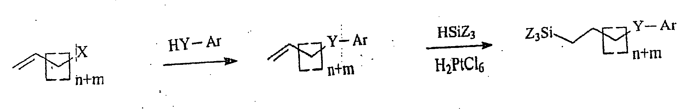
[0072] Compounds having alkyl chains and different substituents in the α- and ω-position are commercially available only up to a chain length of 12 carbon atoms. For longer-chain compounds, ω-bromoalkenes are frequently used starting materials since a large number of simple reactions makes it possible selectively to convert one of the in the case of the functional groups. This is a preparatory step for the synthesis according to the invention, a halogenated 1-alkene then reacts further.

[0073] Heid prepares bromoheptadec-1-ene from the Grignard compound of 5-bromopent-1-ene and an excess of 1,12-dibromododecane using a lithium-copper-catalyzed coupling reaction in 66% yield and made it possible to dispense with the complicated medium-pressure chromatographic purification required in the earlier methods (S. R. Wassermann, Y.-T. Tao, G. M. Whitesides, Langmuir 1989, 5, 1074). Excess starting material and the byproduct docosa-1,21-diene formed from ...

example 1.2

Preparation of (18-Phenoxyoctadecyl)trichlorosilane

[0105] 18-Bromooctadec-1-ene obtained in example 1.1 is now reacted further.

[0106] The following synthesis steps are embodiments for the synthesis method according to the invention, which consists of two synthesis steps. An embodiment comprising both synthesis steps is shown in FIG. 7, both of them being described below.

[0107] In the first synthesis step for the synthesis of octadec-17-enyloxybenzene, potassium phenolate, prepared from phenol and potassium methanolate, is reacted with 18-bromooctadecene (cf. example 1.1) in DMF (N,N-dimethylformamide). After working-up and column filtration, octadec-17-enyloxybenzene was present in reagent grade purity in a yield of 88% for further reaction.

[0108] The trichlorosilane is then synthesized from the alkenyl phenyl ether in the second synthesis step in a platinum-catalyzed hydrosilylation.

[0109] As shown by 1H— and 13C-NMR and mass spectroscopy, this could be obtained in pure form a...

example 2

Preparation of [18-(1′1″-Biphenyl-4′-yloxy)octadecyl]trichlorosilane

[0132] This embodiment of the synthesis method according to the invention is effected analogously to the synthesis of (18-phenoxyoctadecyl)trichlorosilane (example 1.2) starting from 18-bromooctadec-1-ene in two synthesis steps (cf. FIG. 10).

[0133] This is reacted in the first synthesis step in DMF with potassium biphenyl-4-olate, prepared from biphenyl-4-ol and potassium methylate.

[0134] The intermediate 4-octadec-17″-enyloxy-1,1′-biphenyl could be obtained in reagent grade purity in 79% yield after recrystallization from dichloromethane.

[0135] In the second synthesis step, the alkenyl phenyl ether formed as an intermediate is converted in a platinum-catalyzed hydrosilylation into [18-(1′1″-biphenyl-4′-yloxy)-octadecyl]trichlorosilane.

[0136] Since the 4-octadec-17″-enyloxy-1,1′-biphenyl dissolves poorly in trichlorosilane, toluene was added as a cosolvent. After final distillation, pure trichlorosilane was obt...


PUM

PropertyMeasurementUnit
supply voltagesaaaaaaaaaa
thicknessesaaaaaaaaaa
channel lengthaaaaaaaaaa

Abstract

A synthesis method of a compound used to form a self-assembled monolayer used in a semiconductor component is provided. A method includes a first step of replacing a terminal halogen of an ω-haloalk-1-ene with a compound having at least one aromatic group, and a second step of hydrosilylating the reaction product of the first step. Reaction products of the first step include octadec-17-enyloxybenzene, 4-octadec-17″-enyloxy-1,1′-biphenyl, 2-heptadec-16′-enylthiophene, and 2-octadec-17′-enylthiophene. Monolayers provided include 18-phenoxyoctadecyl)trichlorosilane, [18-(1′,1″-biphenyl-4′-yloxy)octadecyl]trichlorosilane, (17-thien-2′-ylheptadecyl)trichlorosilane, (18-thien-2′-yloctadecyl)trichlorosilane, and 4-(18′-trichlorosilyloctadecyloxy)benzonitrile. An organic field effect transistor having monolayers according to embodiments of the invention is provided.

Description

[0001] This application is a continuation of co-pending International Application No. PCT / DE2004 / 001319, filed Jun. 18, 2004, which designated the United States and was not published in English, and which is based on German Application No. 103 28 810.4 filed Jun. 20, 2003, both of which applications are incorporated herein by reference.TECHNICAL FIELD [0002] The invention relates to semiconductor manufacturing and more particularly to organic field effect transistors (OFET) and semiconductor components having organic compounds, organic monolayers, and organic layer structures. BACKGROUND [0003] Increasingly, semiconductor components are being produced using organic materials. For example, field effect transistors based on organic semiconductors (OFET) are of interest for a large number of electronic applications. In particular, low manufacturing costs, flexible or unbreakable substrates or the production of transistors and integrated circuits over large active areas are possible the...

Claims


Application Information

Patent Timeline
Patent Type & Authority Applications(United States)
IPC IPC(8): H01L21/50C07F7/12C07F7/14C08G85/00H01L51/00H01L51/05H01L51/10H01L51/40
CPCB82Y10/00B82Y30/00B82Y40/00C07F7/12H01L51/005H01L51/0068H01L51/0075H01L51/0541H10K85/60H10K85/655H10K85/701H10K10/464H01L21/18
Inventor EFFENBERGER, FRANZSCHUETZ, MARKUSMAISCH, STEFFENSEIFRITZ, STEFFENSCHMID, GUENTERHALIK, MARCUSKLAUK, HAGENZSCHIESCHANG, UTEHOLBERG, STEFAN
Owner QIMONDA
Why Eureka
Try Eureka