
Semiconductor memory device

a semiconductor and memory technology, applied in the direction of semiconductor devices, basic electric elements, electrical appliances, etc., can solve the problems of reducing the electrical characteristics of memory action, etching damage on the side walls of the resistor layer, and troublesome depositing the resistor layer over the stepped, so as to minimize the dependence on the width of the electrode line, the effect of reducing the resistance of unwanted variations and minimizing the resistan

Inactive Publication Date: 2006-07-13
SHARP KK
View PDF10 Cites 39 Cited by
  • Summary
  • Abstract
  • Description
  • Claims
  • Application Information

AI Technical Summary

Benefits of technology

[0021] The present invention has been developed in view of the foregoing aspects and its object is to provide an improve method of manufacturing a semiconductor memory device of the cross point structure in which the memory element material for storage of data is uniform in the crystalline properties while eliminating any damaged layers which are commonly created by the conventional method.
[0030] In the method of manufacturing a semiconductor memory device according to the present invention, the annealing step is provided for eliminating the damaged layer D1 at the surface of the lower electrode lines and thus allows the resistor layer to be deposited as an epitaxial thin film over the lower electrode lines. As the result, variations in the resistance depending largely on the crystalline properties of the resistor layer will be minimized.
[0031] Also, in the method of manufacturing a semiconductor memory device according to the present invention, another annealing step is provided for modifying the resistor layer deposited over the damaged layer D1 at the surface of the lower electrode lines to be equal to the quality of an epitaxial thin film. Equally, unwanted variations in the resistance will be minimized.
[0032] Moreover, in the method of manufacturing a semiconductor memory device according to the present invention, the annealing step is provided for eliminating the damaged layer D2 at the side walls of the resistor layer and thus allows the resistor layer to be deposited uniformly in the properties throughout the cross point areas. Since its dependency on the width of the electrode lines is minimized, the device can be improved in the miniaturization.

Problems solved by technology

It will otherwise be troublesome to deposit the resistor layer over the stepped surface of the lower electrode layer because the selectable ratio of etching between the resistor layer and the lower electrode layer is not applicable in the succeeding resistor layer etching step.
However, there are two drawbacks in the conventional method which will be explained below.
Such nonuniformity in the crystalline orientation will result in variations in the resistance and the rate of resistance change, hence lowering the electrical characteristics in the memory action.
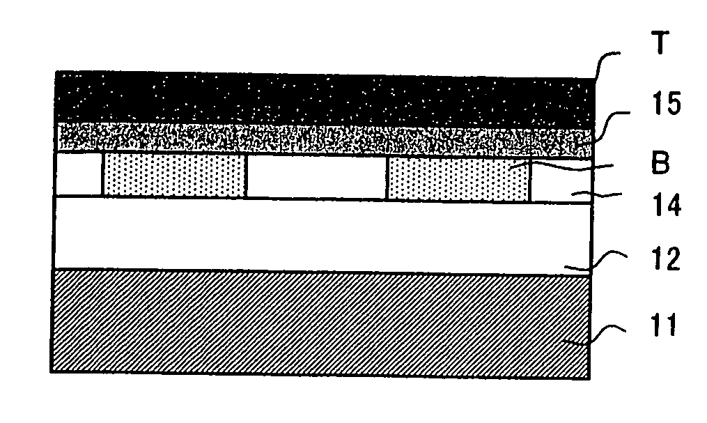
As the second drawback of the conventional method, the action of etching the resistor layer 15, which is commonly implemented by an anisotropic dry etching technique as shown in FIGS. 22A and 22B, may create etching damages on the side walls of the resistor layer 15 with its plasma ions.
Such chemical agents will consequently damage the side walls of the resistor layer 15.
Also, their level may frequently trap electrical charges.
This effect of the damaged layer will make the switching action unstable or decline the degree of data retention.

Method used


Image

  • Semiconductor memory device
  • Semiconductor memory device
  • Semiconductor memory device

Examples


first embodiment

(First Embodiment)

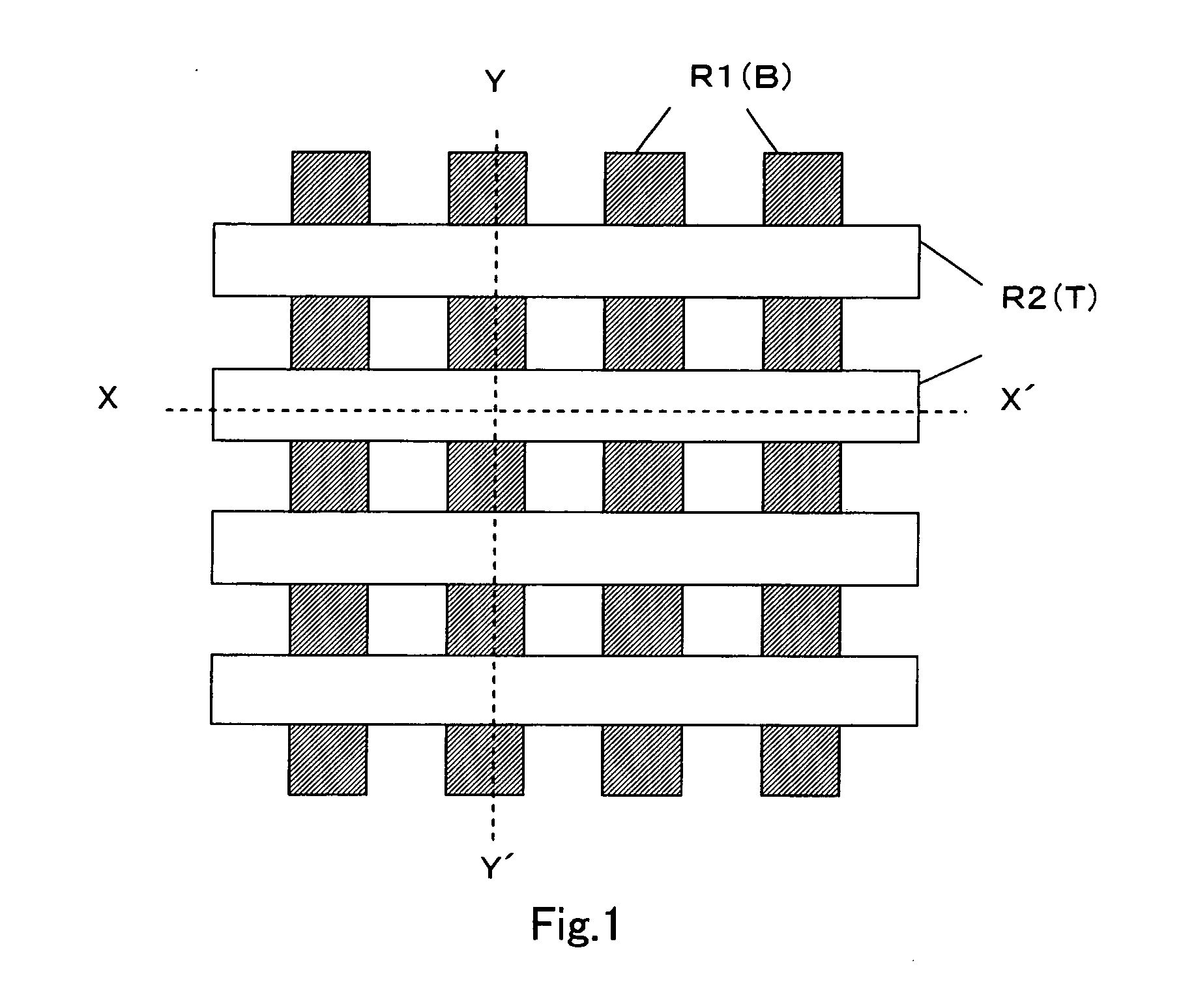
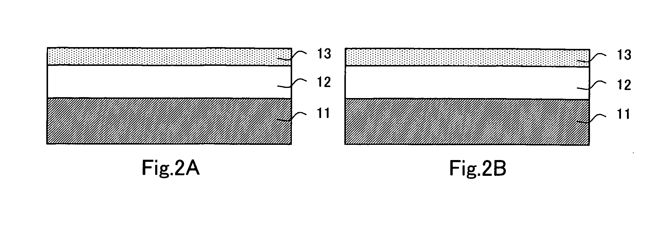
[0060]FIGS. 2A to 7A and FIGS. 2B to 7B illustrate steps of the inventive method showing the first embodiment of the present invention. FIGS. 2A to 7A are vertical cross sectional views taken along the line X-X′ of FIG. 1. Similarly, FIGS. 2B to 7B are vertical cross sectional views taken along the line Y-Y═ of FIG. 1. The term “vertical” in this specification means a direction vertical to the surface of a semiconductor substrate 11 unless otherwise specified.

[0061] The procedure starts with, similar to the conventional method, depositing a BPSG layer 12 to a thickness of 1300 nm, which serves as the interlayer insulating layer under a memory cell, on the silicon semiconductor substrate 11 on which transistor circuits (not shown) are patterned and polishing the same to a thickness of 600 nm by a CMP (chemical mechanical polishing) technique to planarize its surface. Then as shown in FIGS. 2A and 2B, a sputtering step is conducted for depositing a Pt layer 13 (acti...

second embodiment

(Second Embodiment)

[0068] The second embodiment of the inventive method will now be described referring to the relevant drawings. The second embodiment is a modification of the first embodiment and particularly, its step of providing the lower electrode lines B is different from that of the first embodiment. FIGS. 8A to 12A and FIGS. 8B to 12B illustrate steps of the inventive method of the second embodiment. FIGS. 8A to 12A are vertical cross sectional views taken along the line X-X′ of FIG. 1. Similarly, FIGS. 8B to 12B are vertical cross sectional views taken along the line Y-Y′ of FIG. 1.

[0069] The procedure starts with, similar to the conventional method, depositing a BPSG layer 12 to a thickness of 1300 nm, which serves as the interlayer insulating layer under a memory cell, on the silicon semiconductor substrate 11 on which transistor circuits (not shown) are patterned and polishing the same to a thickness of 800 nm by a CMP (chemical mechanical polishing) technique to plana...

third embodiment

(Third Embodiment)

[0074] The third embodiment of the inventive method will then be described referring to the relevant drawings. The third embodiment is a modification of the first or second embodiment and particularly, its annealing step is different in both the order and the purpose from that of the first or second embodiment. FIGS. 13A and 14A and FIGS. 13B and 14B illustrate summary steps of the inventive method of the third embodiment. FIGS. 13A and 14A are vertical cross sectional views taken along the line X-X′ of FIG. 1. Similarly, FIGS. 13B and 14B are vertical cross sectional views taken along the line Y-Y of FIG. 1.

[0075] The procedure starts with the step of providing the lower electrode lines B similar to that of the first or second embodiment and then depositing a resistor (PCMO) layer 15 made of a PCMO material (Pr0.7Ca0.3MnO3) for developing a memory element over the semiconductor substrate provided with the lower electrode lines B or a combination of the lower elec...


PUM


Abstract

The present invention is directed towards a method of manufacturing a semiconductor memory device arranged of a cross point memory array having memory elements provided between upper and lower electrodes for storage of data. The present invention comprises a lower electrode lines forming step of planarizing each of the lower electrode lines and insulating layers provided on both sides of the lower electrode line so as to be substantially uniform in the height thus for patterning the lower electrode lines, a memory element layer depositing step of depositing on the lower electrode lines a memory element layer for the memory elements, and an annealing step of annealing with heat treatment either between the lower electrode lines forming step and the memory element layer depositing step or after the memory element layer depositing step so that any damages caused by the polishing of the surface of the lower electrode lines can be eliminated.

Description

CROSS REFERENCE TO RELATED APPLICATTION [0001] This Nonprovisional application claims priority under 35 U.S.C. §119(a) on Patent Application No. 2005-003799 filed in Japan on Jan. 11, 2005, the entire contents of which are hereby incorporated by reference. BACKGROUND OF THE INVENTION [0002] 1. Field of the Invention [0003] The present invention relates to a method of manufacturing a semiconductor memory device and more particularly to a method of manufacturing a semiconductor memory device arranged of a cross point structure having a plurality of upper electrode lines patterned to extend in one direction, a plurality of lower electrode lines patterned to extend at a right angle to the direction of the upper electrode lines, and memory elements provided between the upper electrode lines and the lower electrode lines for storage of data. [0004] 2. Description of the Related Art [0005] A common semiconductor memory device such as DRAM, NOR flash memory, or FeRAM is arranged in which ea...

Claims


Application Information

Patent Timeline
IPC IPC(8): H01L21/8242
CPCH01L27/2463H01L45/04H01L45/1233H01L45/147H01L45/1641H01L45/1675H10B63/80H10N70/20H10N70/826H10N70/8836H10N70/041H10N70/063
Inventor SHINMURA, NAOYUKIOHNISHI, SHIGEOOHNISHI, TETSUYAYAMAZAKI, SHINOBUSHIBUYA, TAKAHIRONAKANO, TAKASHITAJIRI, MASAYUKI
Owner SHARP KK
Learn More