
Ruthenium layer formation for copper film deposition

a technology of ruthenium layer and copper film, which is applied in the direction of resistive material coating, chemical vapor deposition coating, metallic material coating process, etc., can solve the problems of increasing the current density of such feature, void formation in the conductor, and many conventional deposition process difficulties in filling structures

Inactive Publication Date: 2006-07-13
APPLIED MATERIALS INC
View PDF62 Cites 55 Cited by
  • Summary
  • Abstract
  • Description
  • Claims
  • Application Information

AI Technical Summary

Benefits of technology

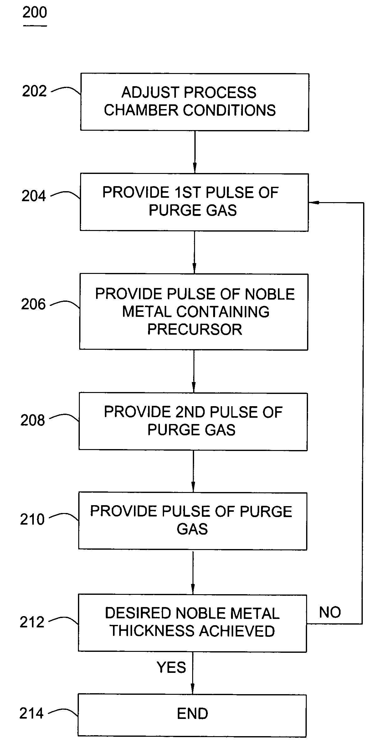
[0012] A method of noble metal layer formation for high aspect ratio interconnect features is described herein. The noble metal layer is formed using a cyclical deposition process, such as atomic layer deposition (ALD). The cyclical deposition process includes alternately adsorbing a noble metal-containing precursor and a reducing gas on a substrate structure. The adsorbed noble metal-containing precursor reacts with the reducing gas to form the noble metal layer on the substrate. Suitable noble metals may include, for example, ruthenium, palladium, platinum, cobalt, nickel, or rhodium.
[0013] The noble metal layer formation is compatible with integrated circuit fabrication processes. In one integrated circuit fabrication process, the noble metal layer may be used as an underlayer for a copper seed layer within a copper interconnect. For such an embodiment, a preferred process sequence includes providing a substrate having an interconnect pattern defined in one or more dielectric layers formed thereon. The interconnect pattern includes a barrier layer conformably deposited thereon. A noble metal layer (e.g., ruthenium) is conformably deposited on the barrier layer. The noble metal layer is deposited using a cyclical deposition process by alternately exposing the substrate to a noble metal-containing gas and a reducing gas. Thereafter, the copper interconnects are completed by depositing a copper seed layer on the noble metal layer and filling the vias with bulk copper metal.
[0014] In one embodiment, a method for forming a film on a substrate is provided which includes positioning the substrate within a process chamber and forming a ruthenium layer on at least a portion of the substrate by sequentially chemisorbing monolayers of a ruthenium-containing compound and a reducing gas on the substrate to form the ruthenium layer.
[0015] In another embodiment, a method for form...

Problems solved by technology

Many conventional deposition processes have difficulty filling structures where the aspect ratio exceeds 6:1, and particularly where the aspect ratio exceeds 10:1.
Additionally, as the feature widths decrease, the device current typically remains constant or increases, which results in an increased current density for such feature.
Aluminum can also suffer from electromigration leading to the formation of voids in the conductor.
Unfortunately, noble metals deposited on high aspect ratio interconnect features using CVD and / or PVD processes generally have poor step coverage (e.g., deposition of a non-continuous material layer).
The poor step coverage for the noble metal material layer may cause the subsequent copper seed layer deposition using an ECP process to be non-uniform.

Method used


Image

  • Ruthenium layer formation for copper film deposition
  • Ruthenium layer formation for copper film deposition
  • Ruthenium layer formation for copper film deposition

Examples


Embodiment Construction

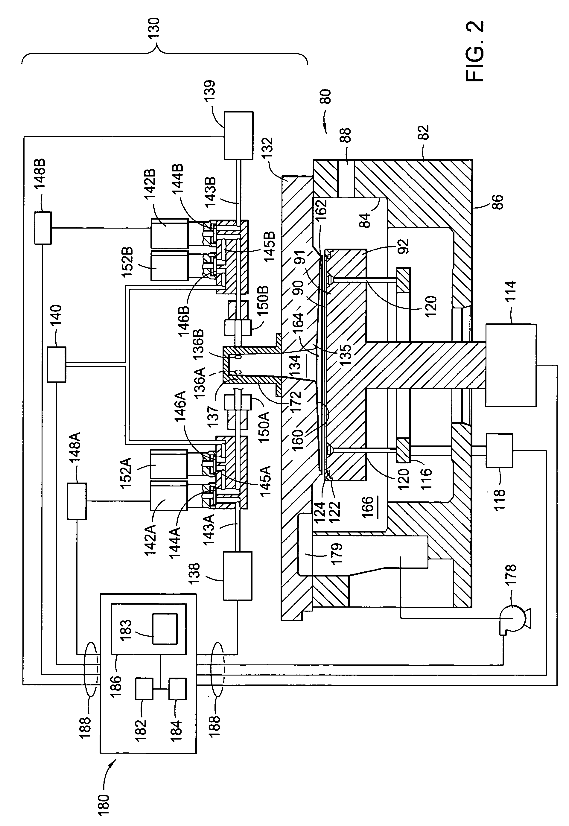
[0024]FIG. 1 depicts a schematic cross-sectional view of a process chamber 10 that can be used to perform integrated circuit fabrication in accordance with embodiments described herein. The process chamber 10 generally houses a substrate support pedestal 48, which is used to support a substrate (not shown). The substrate support pedestal 48 is movable in a vertical direction inside the process chamber 10 using a displacement mechanism 48A.

[0025] Depending on the specific process, the substrate can be heated to some desired temperature prior to or during deposition. For example, the substrate support pedestal 48 may be heated using an embedded heating element 52A. The substrate support pedestal 48 may be resistively heated by applying an electric current from an AC power supply 52 to the heating element 52A. The substrate (not shown) is, in turn, heated by the pedestal 48. Alternatively, the substrate support pedestal 48 may be heated using radiant heaters such as, for example, lamp...


PUM

PropertyMeasurementUnit
Thicknessaaaaaaaaaa

Abstract

In one embodiment, a method for forming a material on a substrate is provided which includes positioning a substrate containing a dielectric material having vias formed therein within a process chamber, forming a barrier layer within the vias and on the dielectric material during a barrier deposition process, forming a ruthenium layer on the barrier layer during a ruthenium deposition process, and filling the vias with a copper material during a copper deposition process. The copper material may be formed by depositing a copper bulk layer over a copper seed layer. The method further provides that the ruthenium layer may be formed by an atomic layer deposition process (ALD) or a physical vapor deposition (PVD) process and the copper material may be formed by an electroless chemical plating process, an electroplating process, a chemical vapor deposition process, an ALD process and / or a PVD process.

Description

CROSS-REFERENCE TO RELATED APPLICATIONS [0001] This application is a continuation of U.S. Ser. No. 10 / 634,662 (APPM / 005975.P1), filed Aug. 4, 2003, which is a continuation-in-part of U.S. Ser. No. 10 / 443,648 (APPM / 005975), filed May 22, 2003, which claims benefit of U.S. Ser. No. 60 / 385,499 (APPM / 005975L), filed Jun. 4, 2002, which are herein incorporated by reference in their entirety.BACKGROUND OF THE INVENTION [0002] 1. Field of the Invention [0003] Embodiments of the invention generally relate to a method for forming noble metal layers, and more particularly to methods for forming ruthenium layers used in copper integration. [0004] 2. Description of the Related Art [0005] Sub-quarter micron, multi-level metallization is one of the key technologies for the next generation of very large scale integration (VLSI) and ultra large scale integration (ULSI) semiconductor devices. The multilevel interconnects that lie at the heart of this technology require the filling of contacts, vias,...

Claims


Application Information

Patent Timeline
IPC IPC(8): B05D5/12C23C28/00H05K3/00C23C28/02B05D3/10C23C16/18C23C16/44C23C16/455H01L21/285H01L21/768
CPCB82Y30/00C23C16/18C23C16/45553H01L21/28562H01L21/76843H01L21/76871H01L21/76873H01L21/76874
Inventor CHANG, MEIGANGULI, SESHADRIMAITY, NIRMALYA
Owner APPLIED MATERIALS INC
Learn More