Method of fabricating a flash memory device

a flash memory device and flash memory technology, applied in the direction of semiconductor devices, basic electric elements, electrical equipment, etc., can solve the problems of rom devices exhibit much higher input/output speeds but are volatile memory devices, and deteriorating the memory function of the flash memory device, so as to prevent over-etching and recessing phenomena, improve process margin, and improve isolation

Inactive Publication Date: 2006-07-06
DONGBU ELECTRONICS CO LTD
View PDF6 Cites 9 Cited by
  • Summary
  • Abstract
  • Description
  • Claims
  • Application Information

AI Technical Summary

Benefits of technology

[0016] An advantage of the present invention is that it can provide a method of fabricating a flash memory device, which improves the isolation between the floating gate and the control gate by patterning the control gate and an ONO layer after sequentially forming a dummy pattern, a source / drain region, a spacer, and an insulating layer.
[0017] Another advantage of the present invention is that it can provide a method of fabricating a flash memory device, which prevents over-etching and recessing phenomena caused during an etching process performed with respect to the ONO layer using a fluorine gas (e.g., CF4), to thereby enable an increased process margin.
[0018] Additional features and advantages of the present invention will be set forth in part in the description which follows, and in part will become apparent from the description, or may be learned by practice of the invention. These and other advantages of the invention may be realized and attained by the structure particularly pointed out in the written description and claims hereof as well as the appended drawings.
[0019] To achieve these and other advantages in accordance with the purpose of the invention, as embodied and broadly described herein, a method of fabricating a flash memory device comprises forming a floating gate on a semiconductor substrate; forming a dummy pattern on the floating gate; etching the floating gate using the dummy pattern as a hard mask; forming an insulating layer flush with an upper surface of the dummy pattern; removing the dummy pattern to leave a space for an ONO layer and control gate formation; and sequentially forming an ONO layer and a control gate in the space left by removing the dummy pattern.
[0020] It is to be understood that both the foregoing general description and the following detailed description of the present invention are exemplary and explanatory and are intended to provide further explanation of the invention as claimed.

Problems solved by technology

While RAM devices, such as a dynamic random access memory (DRAM) or a static random access memory (SRAM), are considered non-volatile since data storage is maintained even if power is interrupted, the input / output speed (access time) of such devices is rather slow.
On the other hand, ROM devices exhibit much higher input / output speeds but are volatile memory devices.
In the above method, however, if the exposed side surfaces of the ONO layer pattern 7a are over-etched, the electrons stored in the floating gate (5a) are provided a path to move into the control gate (9), thereby deteriorating the memory function of the flash memory device and causing an operational instability.
These undesirable phenomena are especially problematic if the ONO layer is etched using a fluorine gas such as CF4.

Method used


Image

  • Method of fabricating a flash memory device
  • Method of fabricating a flash memory device
  • Method of fabricating a flash memory device

Examples


Embodiment Construction

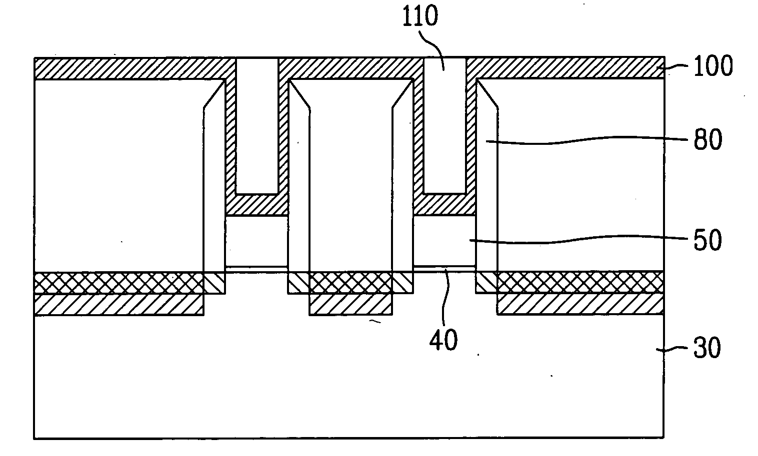
[0026] Reference will now be made in detail to exemplary embodiments of the present invention, examples of which are illustrated in the accompanying drawings. Wherever possible, like reference designations will be used throughout the drawings to refer to the same or similar parts.

[0027] Referring to FIG. 3A, a tunnel oxide layer 40 and a floating gate 50 are sequentially formed on a semiconductor substrate 30. A silicon nitride layer 60 for dummy pattern formation is deposited on the floating gate 50.

[0028] Referring to FIG. 3B, the silicon nitride layer 60 is exposed and etched to form the dummy pattern 60a by photolithography. The silicon nitride layer 60 selectively is etched using a CHxFy gas, for example, CH3F or CH2F2.

[0029] Referring to FIG. 3C, the floating gate 50 is etched using the dummy pattern 60a as a hard mask.

[0030] Referring to FIG. 3D, a source region 70 and a drain region 71 are formed by ion implantation. The source / drain regions 70 and 71 are formed in an ex...


PUM


Abstract

A method of fabricating a flash memory device, having a double gate structure, including an oxide/nitride/oxide (ONO) layer, provides more stable operation by using a dummy pattern upon forming the ONO layer and using a control gate after forming a floating gate. The method includes steps of forming a floating gate on a semiconductor substrate; forming a dummy pattern on the floating gate; etching the floating gate using the dummy pattern as a hard mask; forming an insulating layer flush with an upper surface of the dummy pattern; removing the dummy pattern to leave a space for an ONO layer and control gate formation; and sequentially forming an ONO layer and a control gate in the space left by removing the dummy pattern.

Description

CROSS REFERENCE TO RELATED APPLICATIONS [0001] This application claims the benefit of Korean Patent Application No. 10-2004-0118395, filed on Dec. 31, 2004, which is hereby incorporated by reference as if fully set forth herein. BACKGROUND OF THE INVENTION [0002] 1. Field of the Invention [0003] The present invention relates to a method of fabricating a flash memory device, and more particularly, to a method of fabricating a flash memory device having a double gate structure including an oxide / nitride / oxide (ONO) layer, which has more stable operation by using a dummy pattern upon forming the ONO layer and a control gate after forming a floating gate. [0004] 2. Discussion of the Related Art [0005] A semiconductor memory device may be classified as a read only memory (ROM) devices or a random access memory (RAM) device. While RAM devices, such as a dynamic random access memory (DRAM) or a static random access memory (SRAM), are considered non-volatile since data storage is maintained...

Claims


Application Information

Patent Timeline
Patent Type & Authority Applications(United States)
IPC IPC(8): H01L21/336
CPCH01L21/28273H01L27/115H01L27/11521H01L29/40114H10B69/00H10B41/30H10B99/00
Inventor LEE, KI MIN
Owner DONGBU ELECTRONICS CO LTD
Why Eureka
Try Eureka