Step-down circuit with stabilized voltage

a step-down circuit and stabilized voltage technology, applied in the direction of pulse technique, amplifiers with min 3 electrodes or 2 pn junctions, instruments, etc., can solve the problem that the step-down circuit cannot be installed in the semiconductor integrated circuit devi

Inactive Publication Date: 2006-06-29
RENESAS ELECTRONICS CORP
View PDF11 Cites 6 Cited by
  • Summary
  • Abstract
  • Description
  • Claims
  • Application Information

AI Technical Summary

Benefits of technology

[0008] Further, a constant current source is used to cause a bias current for setting current consumption to flow in each differential amplifying MOSFET. A capacitor is provided between a circuit node responsive to a variation in external power supply voltage, and a ground potential to thereby detect a rise in the external power supply voltage. An operating current of the amplifying MOSFET is increased through the use of a current flowing in the capacitor due to such a variation in external power supply voltage to thereby execute the operation of stabilizing an output voltage corresponding to the rise in the external power supply voltage.

Problems solved by technology

A problem arises in that current consumption allowed for the step-down circuit to realize such low power consumption results in about 120 nA at most, and the step-down circuit cannot be installed in a semiconductor integrated circuit device intended for such low power consumption.

Method used


Image

  • Step-down circuit with stabilized voltage
  • Step-down circuit with stabilized voltage
  • Step-down circuit with stabilized voltage

Examples


Embodiment Construction

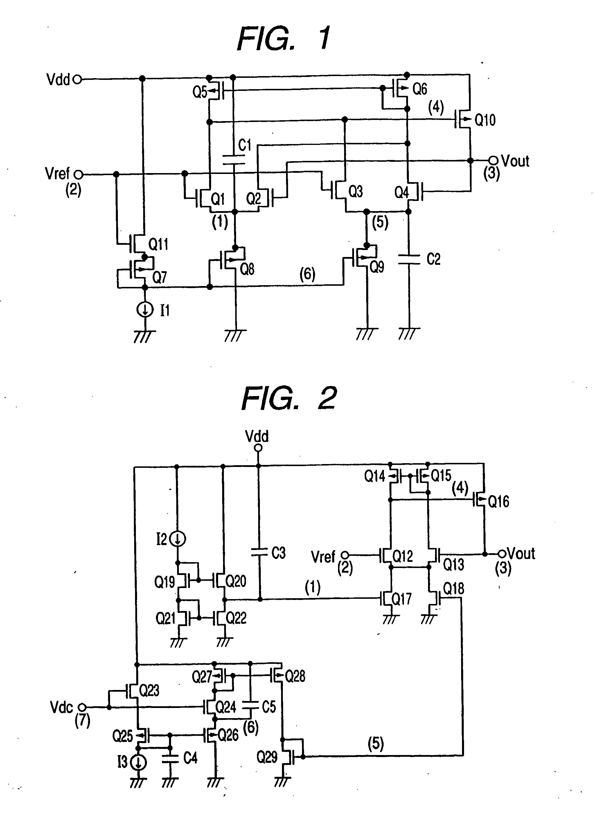
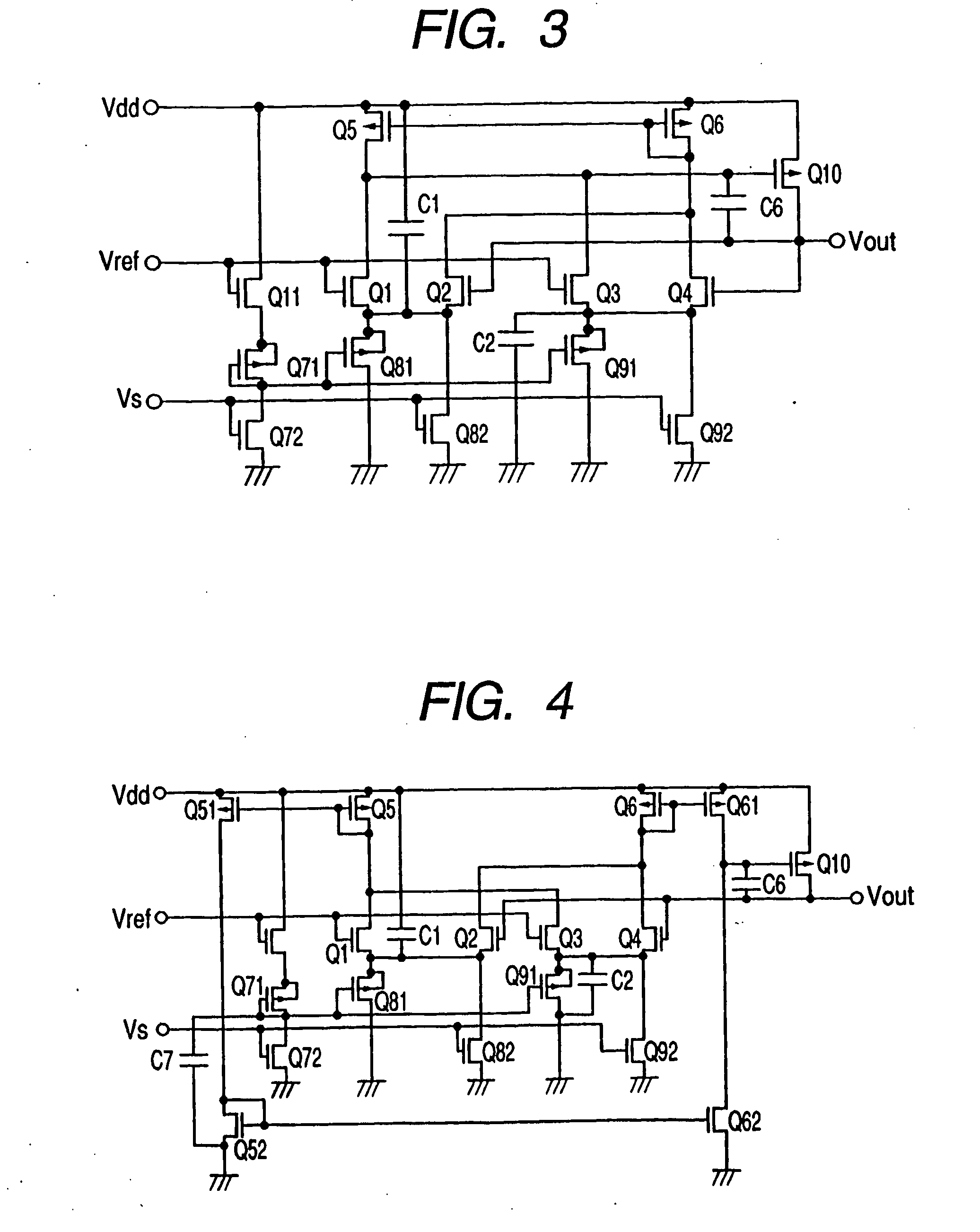
[0031] A circuit diagram of one embodiment of a negative feedback amplifier circuit installed in a semiconductor integrated circuit device according to the present invention is shown in FIG. 1. Respective circuit elements that constitute the present embodiment, are formed on a single substrate by the known CMOS semiconductor manufacturing technology together with other circuit elements that constitute the semiconductor integrated circuit device. The negative feedback amplifier circuit shown in the same drawing comprises a CMOS circuit made up of combinations of N-channel type MOSFETs and P-channel type MOSFETs. The P-channel type MOSFETs are distinguished from the N-channel type MOSFETs by marking their gates (channel portions) with arrows. This is similar even in the case of other circuit diagrams.

[0032] The negative feedback amplifier circuit according to the present embodiment constitutes a voltage follower circuit wherein its output voltage is fed back 100% to thereby power-amp...


PUM


Abstract

The present invention provides a semiconductor integrated circuit device equipped with a negative feedback amplifier circuit or a step-down circuit which realizes stabilization of an output voltage effectively in response to a variation in power supply voltage. A constant current source is used to cause a bias current for setting current consumption to flow in a differential amplifying MOSFET. A capacitor is provided between an external power supply voltage and a predetermined circuit node to thereby detect a reduction in the external power supply voltage. An operating current of the differential amplifying MOSFET is increased through the use of a current flowing in the capacitor due to such an external power variation, thereby executing the operation of stabilizing an output voltage corresponding to the reduction in the external power supply voltage.

Description

CROSS-REFERENCE TO RELATED APPLICATIONS [0001] This application is a Divisional of U.S. application Ser. No. 10 / 960,016 filed on Oct. 8, 2004, which is a Continuation application of U.S. application Ser. No. 10 / 353,013 filed on Jan. 29, 2003, which is a Continuation application of U.S. application Ser. No. 10 / 300,843 filed on Nov. 21, 2002. Priority is claimed based on U.S. application Ser. No. 10 / 960,016 filed on Oct. 8, 2004, which claims priority to U.S. application Ser. No. 10 / 353,013 filed on Jan. 29, 2003, which claims priority to U.S. application Ser. No. 10 / 300,843 filed on Nov. 21, 2002, which claims priority to Japanese Patent Application No. 2001-391235 filed on Dec. 25, 2001.BACKGROUND OF THE INVENTION [0002] The present invention relates to a semiconductor integrated circuit device, and to, for example, a technology effective for application to one equipped with a step-down power circuit for stepping down an external power supply voltage and supplying it to an internal ...

Claims


Application Information

Patent Timeline
Patent Type & Authority Applications(United States)
IPC IPC(8): H03F3/45G05F1/56G11C11/413G05F1/565G11C5/14H01L21/822H01L27/04H03F1/30H03K19/00
CPCG05F1/56G05F1/565G11C5/147H03F2203/45458H03F3/345H03F3/45179H03F2200/513H03F1/34G11C5/14
Inventor SAITOH, YOSHIKAZU
Owner RENESAS ELECTRONICS CORP
Why Eureka
Try Eureka