LOCOS-based junction-pinched schottky rectifier and its manufacturing methods

a manufacturing method and junction pin technology, applied in the direction of diodes, semiconductor devices, electrical apparatus, etc., can solve the problems of forward voltage drop, difficulty in simultaneously obtaining a lower forward voltage drop and a higher reverse breakdown voltage for a conventional schottky barrier diode, and the limited application of trench mos barrier schottky (tmbs) rectifier to low forward curren

Inactive Publication Date: 2006-06-22
SILICON BASED TECH
View PDF1 Cites 23 Cited by
  • Summary
  • Abstract
  • Description
  • Claims
  • Application Information

AI Technical Summary

Benefits of technology

[0010] The present invention discloses a LOCOS-based junction-pinched Schottky (LBJPS) rectifier and its manufacturing methods. The LOCOS-based junction-pinched Schottky (LBJPS) rectifier comprises a raised diffusion guard ring being surrounded by an outer LOCOS field oxide layer, a raised diffusion grid or a plurality of raised diffusion rings or stripes being surrounded by the raised diffusion guard ring, a plurality of recessed semiconductor surfaces being formed on a lightly-doped epitaxial silicon layer surrounded by the raised diffusion grid and the raised diffusion guard ring or by a plurality of raised diffusion rings or stripes and the raised diffusion guard ring, and a metal silicide layer or a metal layer being at least formed on a metal contact region comprising a portion of the raised diffusion guard ring, the plurality of recessed semiconductor surfaces, and the raised diffusion grid or the plurality of raised diffusion rings or stripes. The plurality of recessed semiconductor surfaces are formed by removing a plurality of inner LOCOS field oxide layers. A plurality of compensated diffusion layers can be formed in surface portions of the lightly-doped epitaxial silicon layer under the plurality of recessed semiconductor surfaces. The outer LOCOS field oxide layer and the plurality of inner LOCOS field oxide layers are formed by a local oxidation of silicon (LOCOS) process in a steam or wet oxygen ambient. The plurality of compensated diffusion layers are formed by implanting compensated doping impurities across a pad oxide layer into surface portions of the lightly-doped epitaxial silicon layer in the outer field oxide region (OFOXR) and the plurality of inner field oxide regions (IFOXR) before performing a LOCOS process. The metal contact region is patterned by a masking photoresist step with or without a hard masking layer being formed over an outer portion of a thermal oxide layer formed on the raised diffusion guard ring and a portion of the outer LOCOS field oxide layer.

Problems solved by technology

As a consequence, it is difficult to simultaneously obtain a lower forward voltage drop and a higher reverse breakdown voltage for a conventional Schottky barrier diode.
However, a MOS capacitor formed in the trench grid will exhibit a limited depletion layer extension under a reverse blocking state, so surface area of a Schottky metal contact is small and forward voltage drop is mainly limited by parasitic series resistance of the lightly-doped n− epitaxial silicon layer 112 surrounded by and formed below the trench grid.
As a consequence, the trench MOS barrier Schottky (TMBS) rectifier is limited to low forward current applications.

Method used


Image

  • LOCOS-based junction-pinched schottky rectifier and its manufacturing methods
  • LOCOS-based junction-pinched schottky rectifier and its manufacturing methods
  • LOCOS-based junction-pinched schottky rectifier and its manufacturing methods

Examples


Embodiment Construction

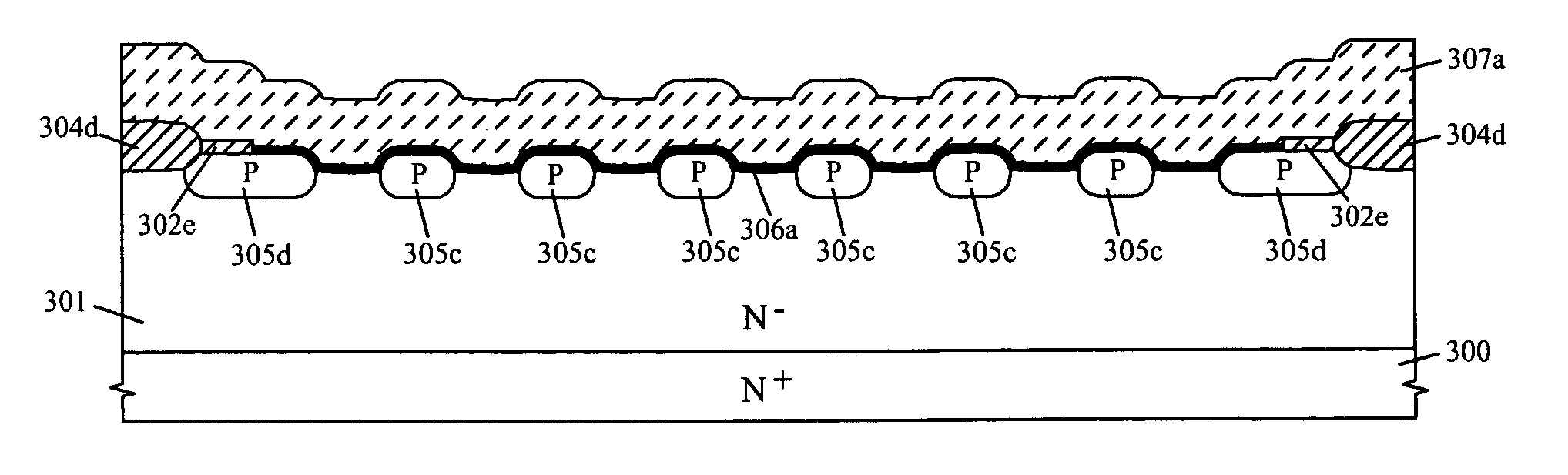
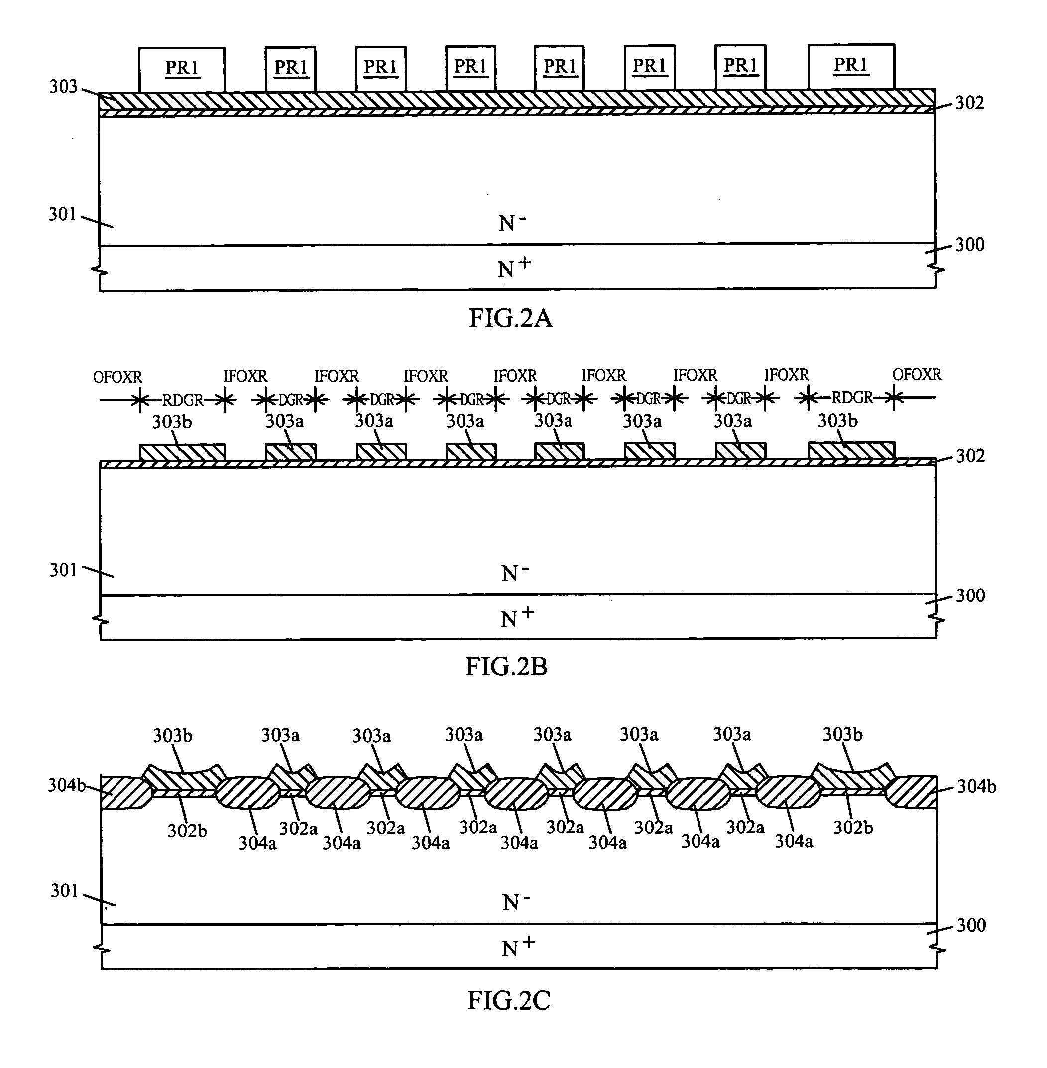
[0016] Referring now to FIG. 2A through FIG. 2F, there are shown process steps and their schematic cross-sectional views of fabricating a first-type LOCOS-based junction-pinched Schottky (LBJPS) rectifier of the present invention.

[0017]FIG. 2A shows that a pad oxide layer 302 is formed on an epitaxial semiconductor substrate 301 / 300 of a first conductivity type; a masking dielectric layer 303 is then formed on the pad oxide layer 302; and subsequently, a first masking photoresist (PRI) step is formed to define a raised diffusion grid region (DGR) and a raised diffusion guard ring region (RDGR). The pad oxide layer 302 is preferably a thermal silicon dioxide layer and has a thickness between 200 Angstroms and 500 Angstroms. The masking dielectric layer 303 is preferably made of silicon nitride as deposited by low-pressure chemical vapor deposition (LPCVD) and its thickness is preferably between 800 Angstroms and 1500 Angstroms. The epitaxial semiconductor substrate 301 / 300 comprises...


PUM


Abstract

The LOCOS-based junction-pinched Schottky rectifier comprises a raised diffusion guard ring surrounded by an outer LOCOS field oxide layer, a raised diffusion grid or a plurality of raised diffusion rings or stripes surrounded by the raised diffusion guard ring, a plurality of recessed semiconductor surfaces formed on a lightly-doped epitaxial semiconductor layer surrounded by the raised diffusion guard ring and the raised diffusion grid or by the raised diffusion guard ring and the plurality of raised diffusion rings or stripes, and a metal silicide layer or a metal layer being at least formed over a portion of the raised diffusion guard ring, the plurality of recessed semiconductor surfaces and the raised diffusion grid or the plurality of raised diffusion rings or stripes. A plurality of compensated diffusion layers can be formed in surface portions of the lightly-doped epitaxial semiconductor layer under the plurality of recessed semiconductor surfaces.

Description

BACKGROUND OF THE INVENTION [0001] 1. Field of the Invention [0002] The present invention relates generally to a Schottky barrier diode (SBD) and its manufacturing method and, more particularly, to a LOCOS-based junction-pinched Schottky (LBJPS) rectifier and its manufacturing methods. [0003] 2. Description of the Related Art [0004] A Schottky barrier diode with a metal-semiconductor contact is known to be a majority carrier diode for high-speed switching and high-frequency rectification. In general, a diffusion guard ring is required for forming the Schottky barrier diode in order to eliminate edge leakage current and soft breakdown due to the metal-semiconductor contact. However, a deeper junction depth of the diffusion guard ring is required to reduce junction curvature effect on reverse breakdown voltage of the Schottky barrier diode. As a consequence, it is difficult to simultaneously obtain a lower forward voltage drop and a higher reverse breakdown voltage for a conventional ...

Claims


Application Information

Patent Timeline
Patent Type & Authority Applications(United States)
IPC IPC(8): H01L27/095H01L29/47H01L29/812H01L31/07H01L31/108
CPCH01L27/0814H01L29/861H01L29/872
Inventor WU, CHING-YUAN
Owner SILICON BASED TECH
Why Eureka
Try Eureka