
Methods for manufacturing silicon wafer and silicon epitaxial wafer, and silicon epitaxial wafer

a technology of epitaxial wafers and manufacturing methods, applied in semiconductor/solid-state device manufacturing, basic electric elements, electric devices, etc., can solve the problems of affecting the ig capability, so as to and improve the ig capability

Inactive Publication Date: 2006-06-22
TAKENO HIROSHI
View PDF13 Cites 8 Cited by
  • Summary
  • Abstract
  • Description
  • Claims
  • Application Information

AI Technical Summary

Benefits of technology

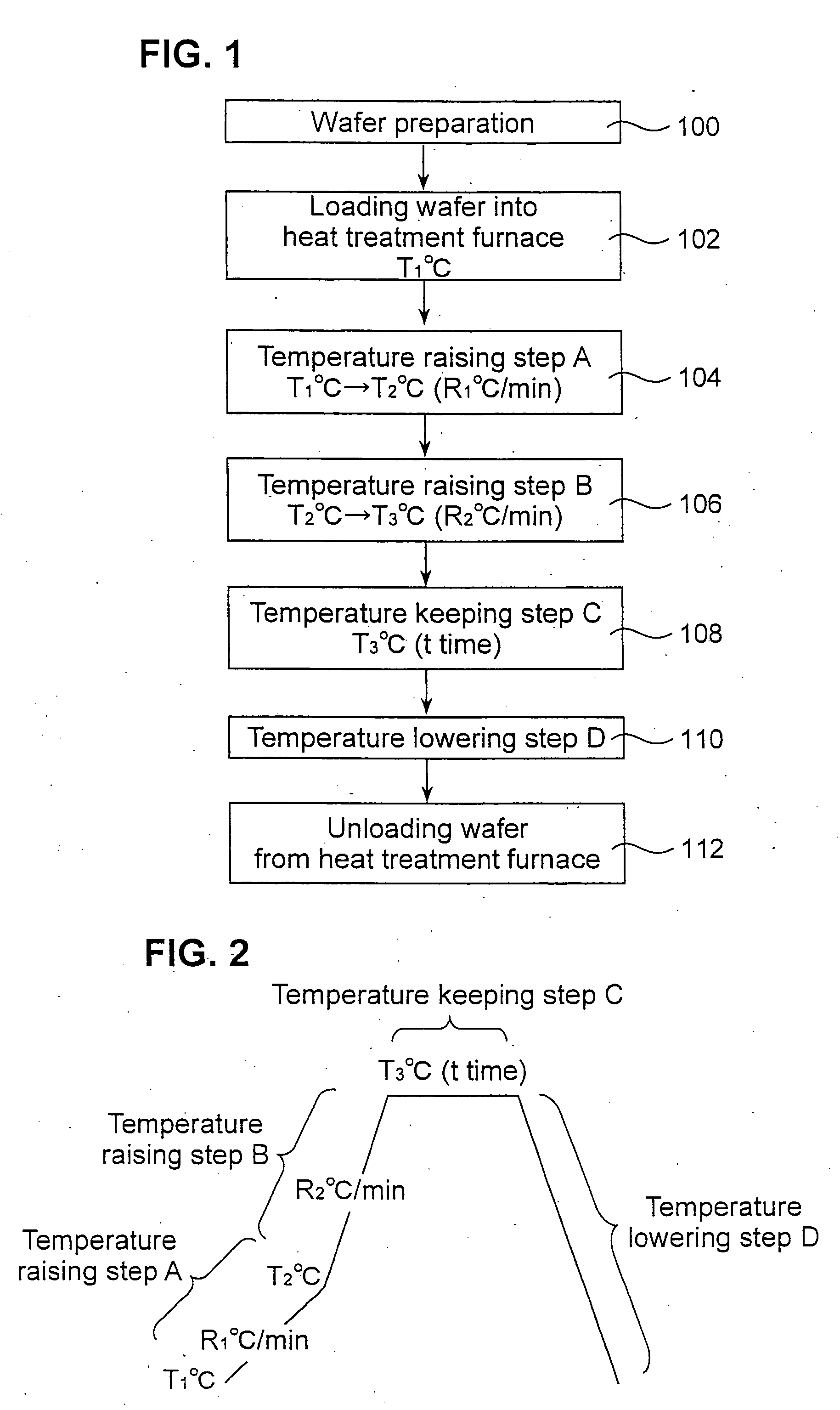
"The present invention provides a method for manufacturing a silicon wafer or a silicon epitaxial wafer that can efficiently form a DZ-IG structure with excellent IG capability in a stable manner. The method involves a temperature raising step A for generating oxygen precipitation nuclei, a temperature raising step B for growing the oxygen precipitation nuclei, and a constant temperature keeping step C for growing the oxygen precipitation nuclei into oxide precipitates of larger sizes. By simultaneously realizing higher density of oxide precipitates and larger sizes of grown-in precipitation nuclei, the method can efficiently form a DZ-IG structure with excellent IG capability in a device fabrication process. The method can also efficiently grow grown-in precipitation nuclei generated in a crystal thermal history in a short time with annihilation being suppressed to the lowest level possible. The method can be used to manufacture silicon wafers with stable IG capability and high efficiency in a lower temperature heat treatment process."

Problems solved by technology

A usual as-grown wafer (a wafer subjected to no heat treatment except for general oxygen donor anihilation heat treatment) has no IG capability because oxygen precipitation nuclei existing at a stage prior to a device fabrication process are extremely small.
Since density of oxygen precipitation nuclei generated during a crystal thermal history depends on the length of the thermal history, there arises a problem that the density is largely fluctuated according to crystal pulling conditions such as a pulling rate or a position in the direction of a crystal growth axis.
On the other hand, when oxide precipitates exist in a device fabrication region in the vicinity of a wafer surface, degradation of the device characteristics occurs.
However, this treatment is long in the total process for heat treatment, resulting in poor efficiency.
When the COPs and voids are present in the device fabrication region, degradation of the device characteristics occurs too.
However, in this case, a problem arises that thermal stress causes slip generation.
However, even when a wafer added with nitrogen is used, there is no change in that it is necessarily subjected to high-temperature heat treatment at about 1200° C. As the wafer diameter becomes larger, the slip more easily generates; therefore especially in a 300 mm wafer that is the mainstream hereafter, there becomes a great problem need of high-temperature heat treatment at about 1200° C. or higher.
Further, since the area where void defects are annihilated is in a very thin surface layer of the order of several μm from the surface, the void defects may degrade device characteristics in a device using a surface layer deeper than the very thin surface layer as a device fabrication region.
Accordingly, in an epi wafer, there arises a problem that an IG capability deteriorates.
Furthermore, the lower the heat treatment temperature is, the smaller the critical size becomes.
However, if the heat treatment temperature is lowered, a growth rate of precipitation nuclei is slowed, so a long time of heat treatment is required for growing the precipitation nuclei to sizes not to be annihilated even in an epi step, which is not preferable because of reduction in productivity.
Furthermore, if there exist oxide precipitates having sizes not to be annihilated even in an epi step, in a recent device fabrication process having a lower temperature and a shorter time, no further growth of the oxide precipitates can be expected in heat treatment of the device fabrication process.

Method used


Image

  • Methods for manufacturing silicon wafer and silicon epitaxial wafer, and silicon epitaxial wafer
  • Methods for manufacturing silicon wafer and silicon epitaxial wafer, and silicon epitaxial wafer
  • Methods for manufacturing silicon wafer and silicon epitaxial wafer, and silicon epitaxial wafer

Examples


examples

[0192] While description will be given of the present invention showing Experimental Examples below, the present invention is not limited to the Experimental Examples.

experimental examples 1 to 5

[0193] There were prepared boron-doped silicon wafers each having a diameter of 8 inches, a plane orientation of and resistivity of about 10 Ω·cm grown by means of a CZ method. Oxygen concentrations of the wafers were 16.0, 17.0, 18.5 and 19.5 ppma, respectively (JEIDA scale). The wafers were all subjected to heat treatment at 1050° C. for 1 hr. With the aid of the heat treatment, almost all oxygen precipitation nuclei formed in a crystal thermal history are annihilated. By this treatment, for example, there can be simulated states of an epi wafer containing almost no oxygen precipitation nuclei and a wafer heat-treated at a temperature of 1000° C. or higher in advance. Note that JEIDA is an abbreviation for Japan Electronic Industry Development Association (now renamed JEITA: Japan Electronics and Information Technology Industries Association).

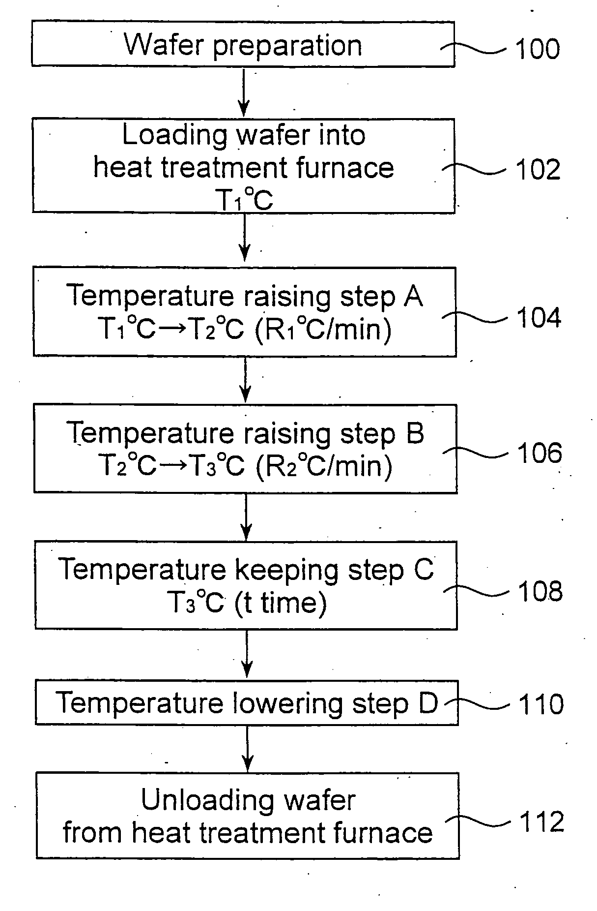
[0194] Next, heat treatment shown in FIGS. 1 and 2 was applied to the wafers. That is, a temperature was raised from T1° C. to T2° C. at a...

experimental examples 6 to 10

[0202] There were prepared mirror-polished silicon wafers each having a diameter of 8 inches, a plane orientation of and resistivity of about 10 Ω·cm, which were manufactured from different two portions (these portions belong to positions grown in the former half and the latter half of the crystal growth step and hereinafter may be referred to as a crystal position A and a crystal position B, respectively) of a boron-doped silicon single crystal grown by means of a CZ method. Oxygen concentrations of the wafers are 16 ppma to 20 ppma (JEIDA scale).

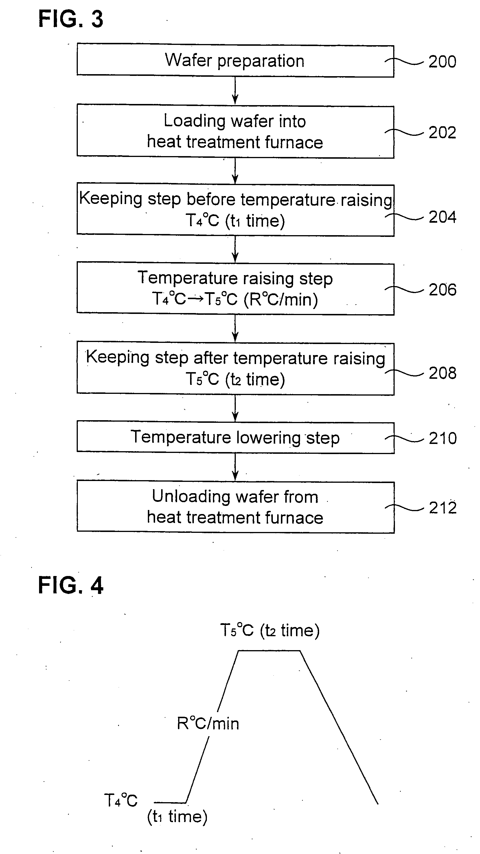
[0203] Next, the wafers were subjected to heat treatment in atmosphere of a mixture of oxygen and nitrogen according to a procedure shown in FIGS. 3 and 4. That is, the wafer was kept at T4° C. for t1 time, thereafter the temperature was raised from the T4° C. to T5° C. at a rate of R° C. / min and kept at the T5° C. for t2 time. After the keeping, the temperature in a heat treatment furnace was lowered to 700° C. at a rate of 2° C. / min an...


PUM

PropertyMeasurementUnit
temperatureaaaaaaaaaa

Abstract

There is provided a method for manufacturing a silicon wafer or a silicon epitaxial wafer capable of imparting an excellent IG capability thereto in a stable manner by simultaneously realizing higher density of oxide precipitates and larger sizes thereof at a stage prior to a device fabrication process. The present invention is a method for manufacturing a silicon wafer wherein the silicon wafer is subjected to heat treatment to impart a gettering capability thereto comprising at least the following three steps of: a temperature raising step A for generating oxygen precipitation nuclei; a temperature raising step B for growing the oxygen precipitation nuclei; and a constant temperature keeping step C for growing the oxygen precipitation nuclei into oxide precipitates of larger sizes.

Description

TECHNICAL FIELD [0001] The present invention relates to methods for manufacturing a silicon wafer and a silicon epitaxial wafer capable of obtaining the silicon wafer and the silicon epitaxial wafer having a defect-free layer (a DZ layer or an epitaxial layer) in the vicinity of a surface thereof and oxide precipitates high in gettering capability in the bulk thereof through heat treatment with extreme efficiency and simplicity, and a silicon epitaxial wafer. BACKGROUND ART [0002] Most of silicon wafers used widely as substrates of semiconductor devices are manufactured from a silicon single crystal grown in a Czochralski (CZ) method. The silicon single crystal grown in the CZ method contains interstitial oxygen as impurities at concentration of about 1018 atoms / cm3. The interstitial oxygen turns into a supersatulated state in a thermal history from solidification of a melt till cooling down thereof to room temperature during a crystal growth step (hereinafter which may be referred ...

Claims


Application Information

Patent Timeline
Patent Type & Authority Applications(United States)
IPC IPC(8): H01L21/322H01L21/44
CPCH01L21/3225H01L21/322
Inventor TAKENO, HIROSHI
Owner TAKENO HIROSHI
Learn More