
Magnetoresistant device and magnetic memory device further comments

a magnetic memory device and magnetic resistance technology, applied in the field of magnetic resistance devices and magnetic memory devices further, can solve the problems of increasing coercivity of tmr devices, slow write speed of second, and inability to write many times, so as to improve the rectangle properties of resistance-magnetic field curves, reduce coercivity, and improve the effect of resistance resistance resistan

Inactive Publication Date: 2006-06-15
SONY CORP
View PDF6 Cites 43 Cited by
  • Summary
  • Abstract
  • Description
  • Claims
  • Application Information

AI Technical Summary

Benefits of technology

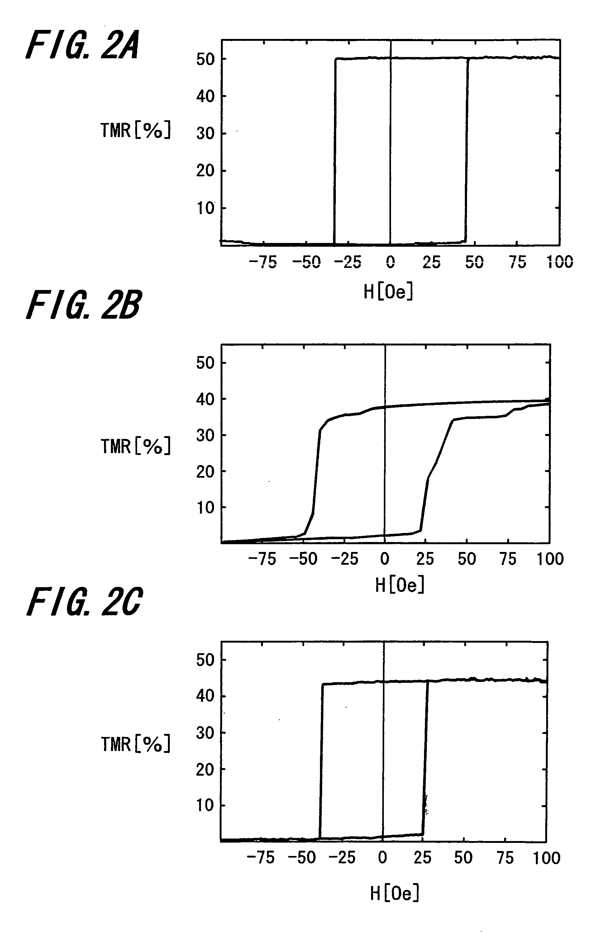
[0029] According to the above-mentioned arrangement of the magnetoresistive device of the present invention, since the pair of ferromagnetic layers is composed of the magnetization fixed layer made of the crystalline ferromagnetic layer provided under the intermediate layer and the magnetization free layer made of the amorphous ferromagnetic layer provided above the intermediate layer, the coercivity can be decreased by the magnetization free layer made of the amorphous ferromagnetic layer, the rectangle properties of the resistance-magnetic field curve can be improved, the bias voltage dependence of the variations in magnetoresistance can be improved and the dispersions of the coercivity can be decreased.
[0030] Further, since the magnetization fixed layer made of the crystalline ferromagnetic layer is provided under the intermediate layer, it becomes possible to realize the high variations in magnetoresistance.
[0031] According to the above-mentioned arrangement of the magnetic memory apparatus of the present invention, since the magnetic memory apparatus includes the magnetoresistive device and the word line and the bit line sandwiching the magnetoresistive device in the thickness direction wherein the magnetoresistive device has the arrangement of the above-described magnetoresistive device of the present invention, the rectangle properties of the resistance-magnetic field curve of the magnetoresistive device can be increased, the bias voltage and the dispersion of the coercivity can be decreased. As a result, the asteroid characteristic of the magnetoresistive device can be improved and it becomes possible to selectively write information in the magnetic memory apparatus with ease stably. That is, the write characteristic can be increased and hence the write error can be decreased.
[0032] Also, since it becomes possible to increase the variation in magnetoresistance of the magnetoresistive device, when information is read out from the magnetic memory apparatus, it becomes easy to discriminate the low resistance state and the high resistance state from each other. As a consequence, the read characteristic can be improved and hence the read error can be decreased.

Problems solved by technology

However, the flash memory encounters with a defect in which its write speed is slow in the order of μsecond.
On the other hand, in the FRAM, a problem is pointed out in which it cannot be rewritten many times.
Also, there arises a problem of heat generated by a write electric current, and from a standpoint of decreasing power consumption, it is necessary to decrease this write electric current.
However, when the TMR device is microminiaturized in order to increase a recording density of the MRAM, for example, there occurs a disadvantage that the coercivity of the TMR device will increase.
Also, if magnetic properties of the TMR device are changed at every device in the MRAM or magnetic properties are changed when the same device is used repeatedly, there arises a problem in which it becomes difficult to selectively write information in the device by using the asteroid characteristic.

Method used


Image

  • Magnetoresistant device and magnetic memory device further comments
  • Magnetoresistant device and magnetic memory device further comments
  • Magnetoresistant device and magnetic memory device further comments

Examples


Embodiment Construction

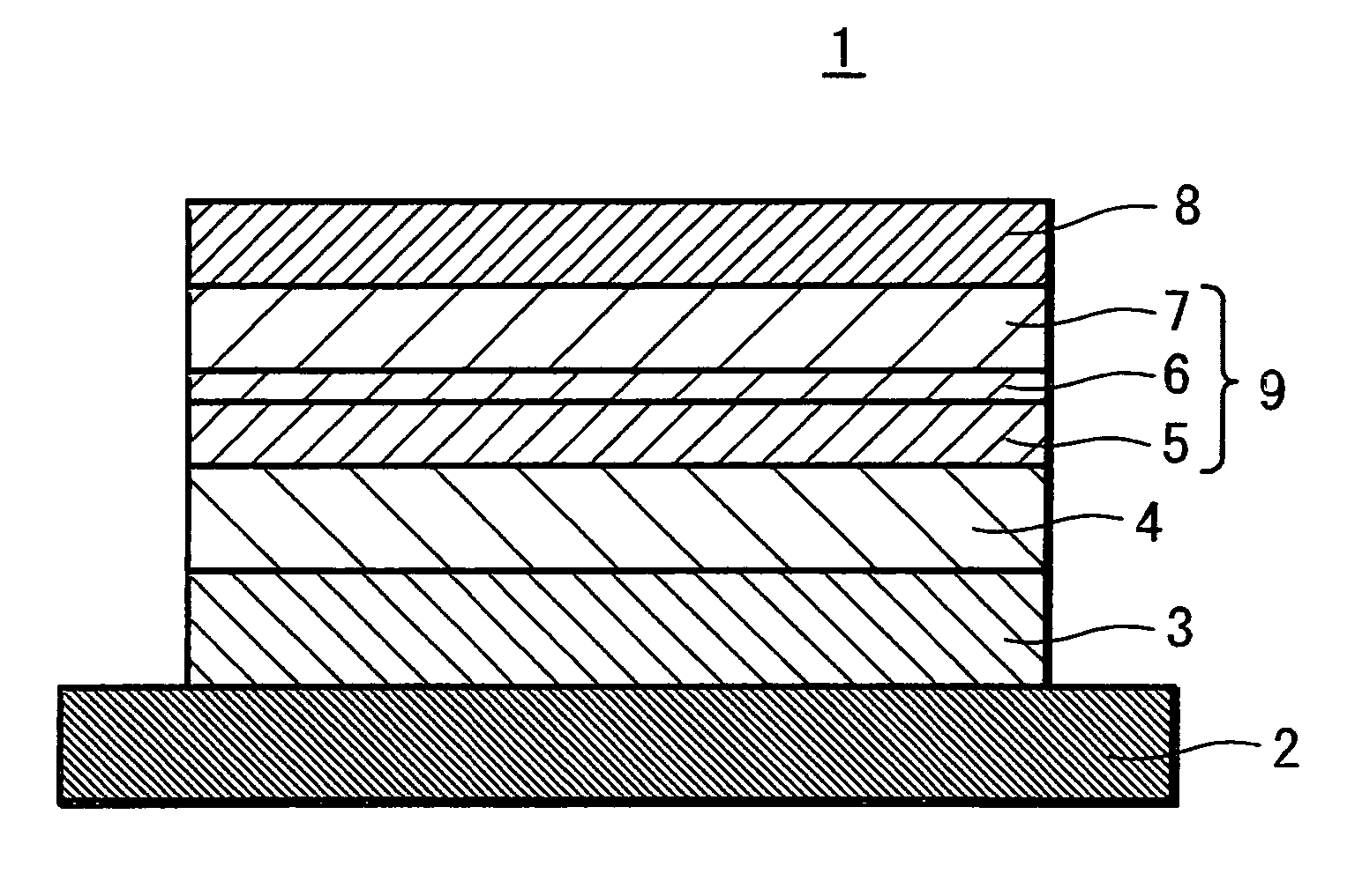
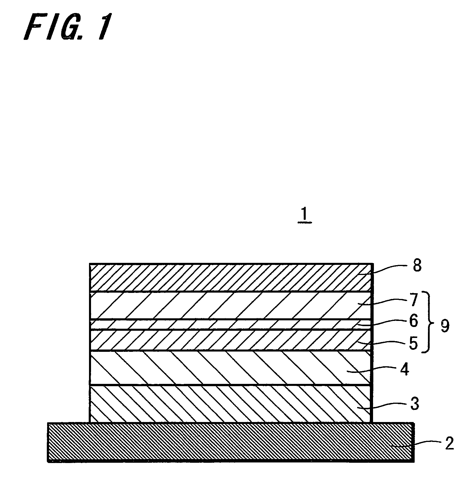
[0040] According to the present invention, in a magnetoresistive device comprising a pair of ferromagnetic layers opposed to each other through an intermediate layer to obtain variations in magnetoresistance with application of an electric current flowing through the direction perpendicular to the film plane, a magnetoresistive device comprises, of the pair of ferromagnetic layers, a magnetization fixed layer composed of a crystalline ferromagnetic layer formed under the intermediate layer and a magnetization free layer composed of an amorphous ferromagnetic layer formed above the intermediate layer.

[0041] Also, according to the present invention, in the above-described magnetoresistive device, the magnetoresistive device has a laminated ferri structure.

[0042] Also, according to the present invention, in the above-described magnetoresistive device, the magnetoresistive device is a tunnel magnetoresistive device using a tunnel barrier layer made of an insulating material or a semic...


PUM


Abstract

There are provided a magnetoresistive device having excellent magnetic properties and a magnetic memory apparatus including this magnetoresistive device and which has excellent read and write characteristics. A magnetoresistive device has an arrangement including a pair of ferromagnetic layers (magnetization fixed layer 5 and magnetization free layer 7) being opposed to each other through an intermediate layer 6 to obtain variations in magnetoresistance by an electric current flowing in the direction perpendicular to the film plane. This magnetoresistive device 1 has the pair of ferromagnetic layers 5, 7 composed of the magnetization fixed layer 5 made of a crystalline ferromagnetic layer provided under the intermediate layer 6 and the magnetization free layer 7 being made of an amorphous ferromagnetic layer being provided above the intermediate layer 6, and the magnetic memory apparatus is composed of this magnetoresistive device 1 and a bit line and a word line sandwiching the magnetoresistive device 1 in the thickness direction.

Description

TECHNICAL FIELD [0001] The present invention relates to a magnetoresistive device having an arrangement to obtain variations in magnetoresistance by an electric current flowing through the direction perpendicular to the film plane and a magnetic memory apparatus including such a magnetoresistive device. BACKGROUND ART [0002] As personal small equipment such as information communication equipment, in particular, personal terminal equipment, are making great progress, devices such as memories and logic devices comprising personal small equipment should be requested to become higher in performance such as they should be higher in integration degree, they should be operated at higher speed and they should save much more electric power. In particular, technologies for increasing density and storage capacity of a nonvolatile memory are becoming as more important replacements of a hard disk and an optical disc which cannot be essentially miniaturized because they have movable portions. [00...

Claims


Application Information

Patent Timeline
IPC IPC(8): H01L43/00H01L29/82H01L27/105G01R33/09G11B5/39G11C11/16H01L21/8246H01L27/22H01L43/08
CPCB82Y10/00B82Y25/00G01R33/093G11B5/3903G11B5/3909G11C11/16H01L27/228H01L43/08H10B61/22H10N50/10
Inventor OHBA, KAZUHIROHOSOMI, MASANORIBESSHO, KAZUHIROMIZUGUCHI, TETSUYAHIGO, YUTAKAYAMAMOTO, TETSUYASONE, TAKEYUKIKANG, HIROSHI
Owner SONY CORP
Learn More