Semiconductor device
a technology of semiconductor devices and semiconductors, applied in semiconductor devices, semiconductor/solid-state device details, electrical apparatus, etc., can solve the problems of high manufacturing method difficulty, resistance of copper wiring rise, and inability to solve problems, etc., to improve the em tolerance of wiring structure and improve the adhesion
- Summary
- Abstract
- Description
- Claims
- Application Information
AI Technical Summary
Benefits of technology
Problems solved by technology
Method used
Image
Examples
second embodiment
(2) Second Embodiment
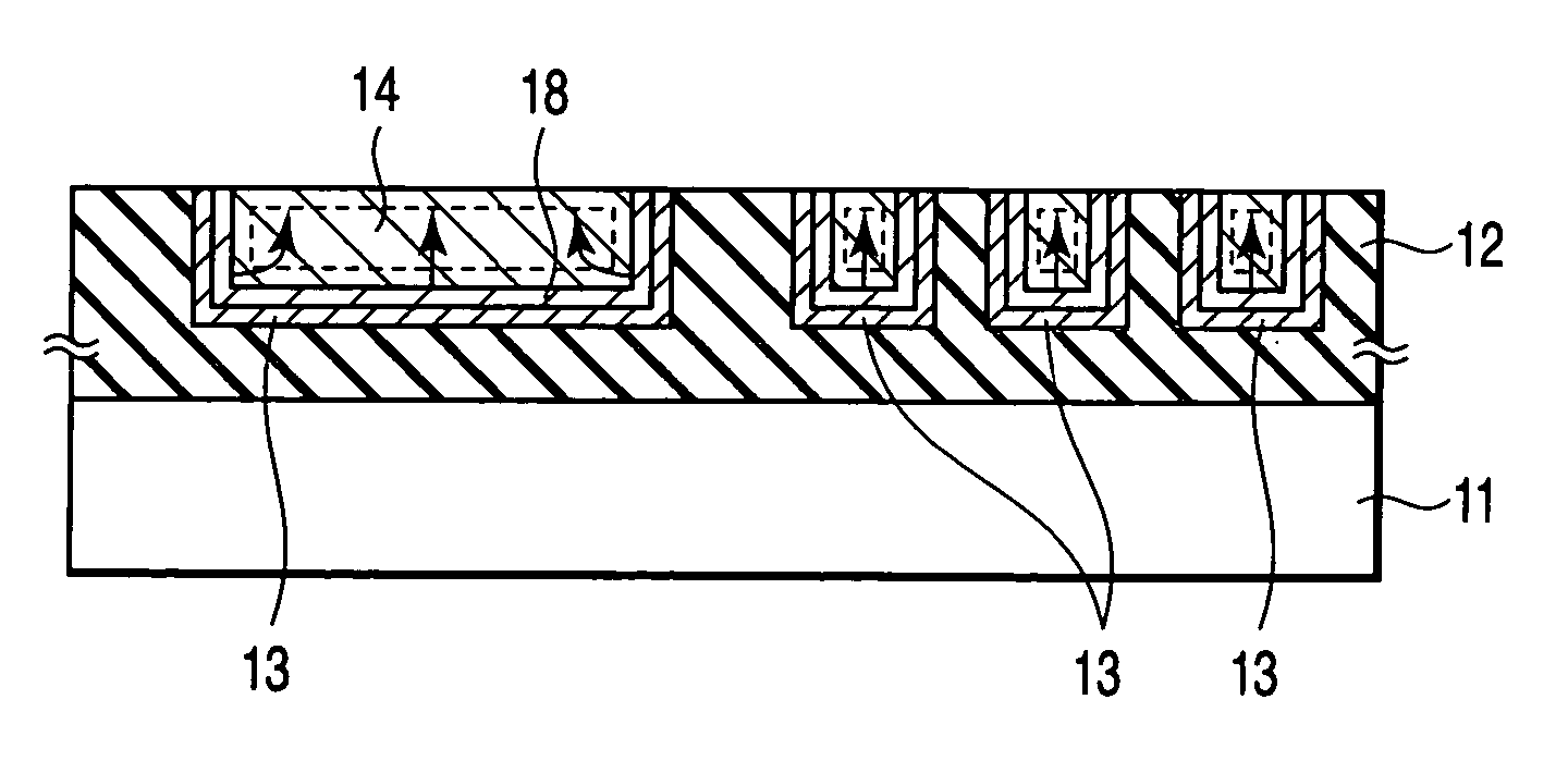
[0068] FIGS. 14 to 17 show a manufacturing method for a semiconductor device according to a second embodiment of the present invention.
[0069] First, as shown in FIG. 14, a wiring slot is formed on the insulating layer (for example, silicon oxide) 12 on the silicon substrate 11 by using a method such as, for example, PEP or RIE.
[0070] The barrier metal 13 for covering the bottom surfaces and the side surfaces of the wiring slot is formed on the insulating layer 12 by using a method such as a CVD method or a PVD method.
[0071] Thereafter, a layer 18 of a material solid-soluble in copper made of an additive which is fused in a solid state in copper, and by which the adhesion with the barrier metal 13 and a stopper (an insulating layer of SiN, SiCN, SiCO, SiC or the like) which will be described later can be improved, for example, Ti, Al, Si, Co, B or P, or the layer 18 of a material solid-soluble in copper including one of those additives is formed on the barrier...
PUM
 Abstract
Description
Claims
Application Information
 - R&D
- Intellectual Property
- Life Sciences
- Materials
- Tech Scout
- Unparalleled Data Quality
- Higher Quality Content
- 60% Fewer Hallucinations
Browse by: Latest US Patents, China's latest patents, Technical Efficacy Thesaurus, Application Domain, Technology Topic, Popular Technical Reports.
© 2025 PatSnap. All rights reserved.Legal|Privacy policy|Modern Slavery Act Transparency Statement|Sitemap|About US| Contact US: help@patsnap.com


