Advanced multi-bit magnetic random access memory device

Active Publication Date: 2006-04-27
SAMSUNG ELECTRONICS CO LTD
View PDF10 Cites 6 Cited by
  • Summary
  • Abstract
  • Description
  • Claims
  • Application Information

AI Technical Summary

Benefits of technology

[0027] According to an aspect of the present invention, an advanced multi-bit magnetic random access memory and a method for writing to the multi-bit magnetic random access memory that improves the memory density of MRAM, and also simplifies the memory fabrication process by reducing the number of electrical current lines.
[0030] According to another aspect of the present invention, a memory is provided that allows for fast and efficient switching. This may be accomplished by spin precessional switching. Except for high operation frequencies, spin precessional switching is energy efficient because it requires a lower switching field as compared to the aforementioned quasistatic writing process. Shorter field pulses further reduce power consumption.
[0036] A fast rising magnetic field pulse applied orthogonal to the M direction will generate a large torque, γ(M×Heff). As a result, M is excited into precession around the effective field direction. The first term in the LLG equation is the precession term, which describes the spin precession, and the second term is the energy dissipation term that dictates the rate of energy dissipation. Adapting spin precessional switching promises high-energy efficiency as well as an ultrafast switching speed.

Problems solved by technology

This method of writing is also known as the quasistatic writing which is not only slow, but also not energy efficient.
Also, in such a memory having a multilayer cell structure, there is a limitation of memory density.
The writing method, however, relies on a quasistatic writing method which is not only slow, but also not energy efficient.
As noted above, this method of switching is not only slow, but also not energy efficient.
Further, the reading process of the Tehrani et al. device is very complex since six magnetic fields are required to determine the state in each data layer separately.
This creates a slow and inefficient reading process.
This means that if this device is to be used for additional data layers, each data layer requires one pair of antiferromagnetic layers, providing for a complicated device structure.
Further, the manufacturing process of related art MRAM devices has only been known to produce low yields of the memory due to high sensitivity to cell defects, which causes domain nucleation, and hence, wide switching field distribution.

Method used


Image

  • Advanced multi-bit magnetic random access memory device
  • Advanced multi-bit magnetic random access memory device
  • Advanced multi-bit magnetic random access memory device

Examples


Embodiment Construction

[0053] Hereinafter, exemplary embodiments of the present invention will be described in detail with reference to the accompanying drawings.

[0054] Aspects of the present invention, and methods for achieving them will be apparent to those skilled in the art from the detailed description of the exemplary embodiments together with the accompanying drawings. However, the scope of the present invention is not limited to the exemplary embodiments disclosed in the specification, and the present invention can be realized in various types. The described exemplary embodiments are presented only for completely disclosing the present invention and helping those skilled in the art to completely understand the scope of the present invention, and the present invention is defined only by the scope of the claims.

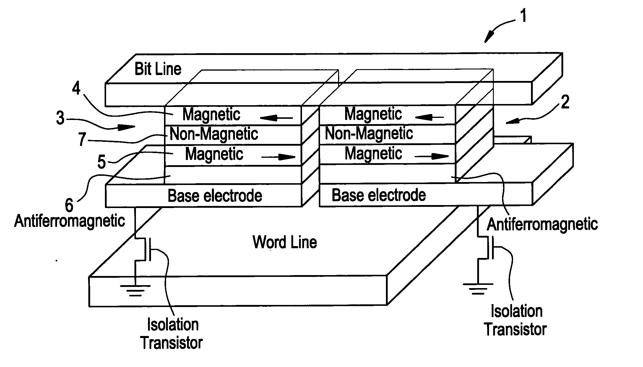
[0055] In a first exemplary embodiment of the invention, a multi-bit MRAM is created by a pair of spin-excitation-field-polarity dependent memory cells. The pair of memory cells (a pair-cel...


PUM


Abstract

An advanced multi-bit magnetic random access memory device and a method for writing to the advanced multi-bit magnetic random access memory device. The magnetic memory includes one or more pair-cells. A pair-cell is two memory cells. Each memory cell has a magnetic multilayer structure. The structure includes a magnetically changeable ferromagnetic layer, a ferromagnetic reference layer having a non-changeable magnetization state, and a corresponding spacer layer separating the ferromagnetic layers. The memory cells are arranged such that an effective remnant magnetization of each of the cells is non-parallel from the cells' long-axis. This allows for more than one-bit to be stored as well as for efficient writing and reduced power consumption.

Description

CROSS-REFERENCE TO RELATED APPLICATIONS [0001] This application claims priority from Korean Patent Application No. 2004-0086392 filed Oct. 27, 2004, the contents of which are incorporated herein by reference in their entirety. BACKGROUND OF THE INVENTION [0002] 1. Field of the Invention [0003] The present invention relates to magnetic random access memory, and more particularly to an advanced multi-bit magnetic random access memory device and a method for writing to the advanced multi-bit magnetic random access memory device. [0004] 2. Description of the Related Art [0005] Rapid growth in digital information generation is likely to face a new wave of explosion in high density memory demand due to the growing popularity of mobile devices. Magnetic random access memory (MRAM) is one of the most promising candidates to provide energy efficient and non-volatile memories. [0006] The most attractive advantages of MRAM are that the mobile device retains the current state of work when power...

Claims


Application Information

Patent Timeline
IPC IPC(8): G11C11/14
CPCG11C11/16G11C11/5607
Inventor LIM, CHEE-KHENG
Owner SAMSUNG ELECTRONICS CO LTD
Why Eureka
Try Eureka