
Dielectric plug in mosfets to suppress short-channel effects

a dielectric plug and short-channel technology, applied in the direction of basic electric elements, electrical apparatus, semiconductor devices, etc., can solve the problems of less power consumption in their operation, lower turn-on threshold voltage, and faster switching speed, so as to reduce short-channel effects, increase source-drain junction capacitance, and reduce short-channel effects.

Inactive Publication Date: 2006-04-13
MICRON TECH INC
View PDF27 Cites 13 Cited by
  • Summary
  • Abstract
  • Description
  • Claims
  • Application Information

AI Technical Summary

Benefits of technology

This approach effectively reduces short-channel effects, lowers threshold voltage, enhances on / off current ratios, and minimizes junction leakage, while allowing for deeper source / drain junctions and improved scalability of MOS devices without increasing capacitance.

Problems solved by technology

Further, smaller transistors typically have lower turn-on threshold voltages, faster switching speeds, and consume less power in their operation.
However, these techniques must contend with problems resulting from higher density itself Even the most advanced processing techniques cannot in all instances offset the problems associated with small features or features arranged extremely close to one another.
For example, as the channel length (distance between source and drain regions) decreases, short-channel effects (SCEs) generally occur, which can result in increased sub threshold leakage, and can become exaggerated when dimensions of the transistor and the channel region is decreased.
Such a condition may be due to avalanche breakdown or punch through.
This is due to the fact that under such conditions, the normal doping concentration of the channel region is not sufficient to prevent flow between the source and drain regions.
Unfortunately, the punch through stop implant also raises the doping concentration of the substrate in the source and drain region.
However, the above-described process can require extreme fine-tuning of process control parameters during dry etching to form the dielectric plugs.
This requirement of a fine control on the process parameters during fabrication of the dielectric plugs can result in uncontrolled position, height, and thickness of the formed dielectric plugs, which are critical to reducing SCEs.
This can also result in uncontrolled channel length and not connecting to source / drain regions to low doping drain (LDD) regions, also referred to as “Source / Drain extensions.” In addition, Silicon / Nitride used in forming the dielectric plugs during the dry etching process, can result in having a poor bonding with the silicon substrate, which can further result in traps and junction leakage.

Method used


Image

  • Dielectric plug in mosfets to suppress short-channel effects
  • Dielectric plug in mosfets to suppress short-channel effects
  • Dielectric plug in mosfets to suppress short-channel effects

Examples


Embodiment Construction

[0022] In the following detailed description, reference is made to various specific embodiments in which the invention may be practiced. These embodiments are described with sufficient detail to enable those skilled in the art to practice the invention, and it is to be understood that other embodiments may be employed, and that structural, logical, electrical, and process changes may be made without departing from the teachings of the invention.

[0023] In the foregoing description of the preferred embodiments, various features of the invention are grouped together in a single embodiment for the purpose of streamlining the disclosure. This method of disclosure is not to be interpreted as reflecting an intention that the claimed invention requires more features than are expressly recited in each claim. Rather, as the following claims reflect, inventive aspects lie in less than all features of a single disclosed embodiment. Thus, the following claims are hereby incorporated into the de...


PUM


Abstract

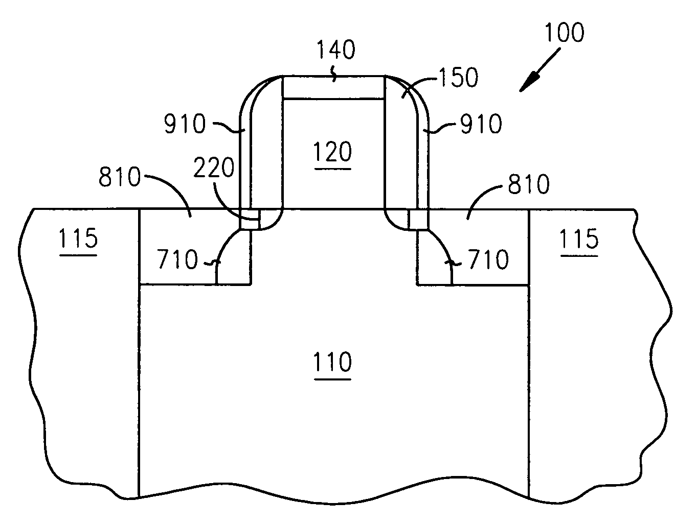
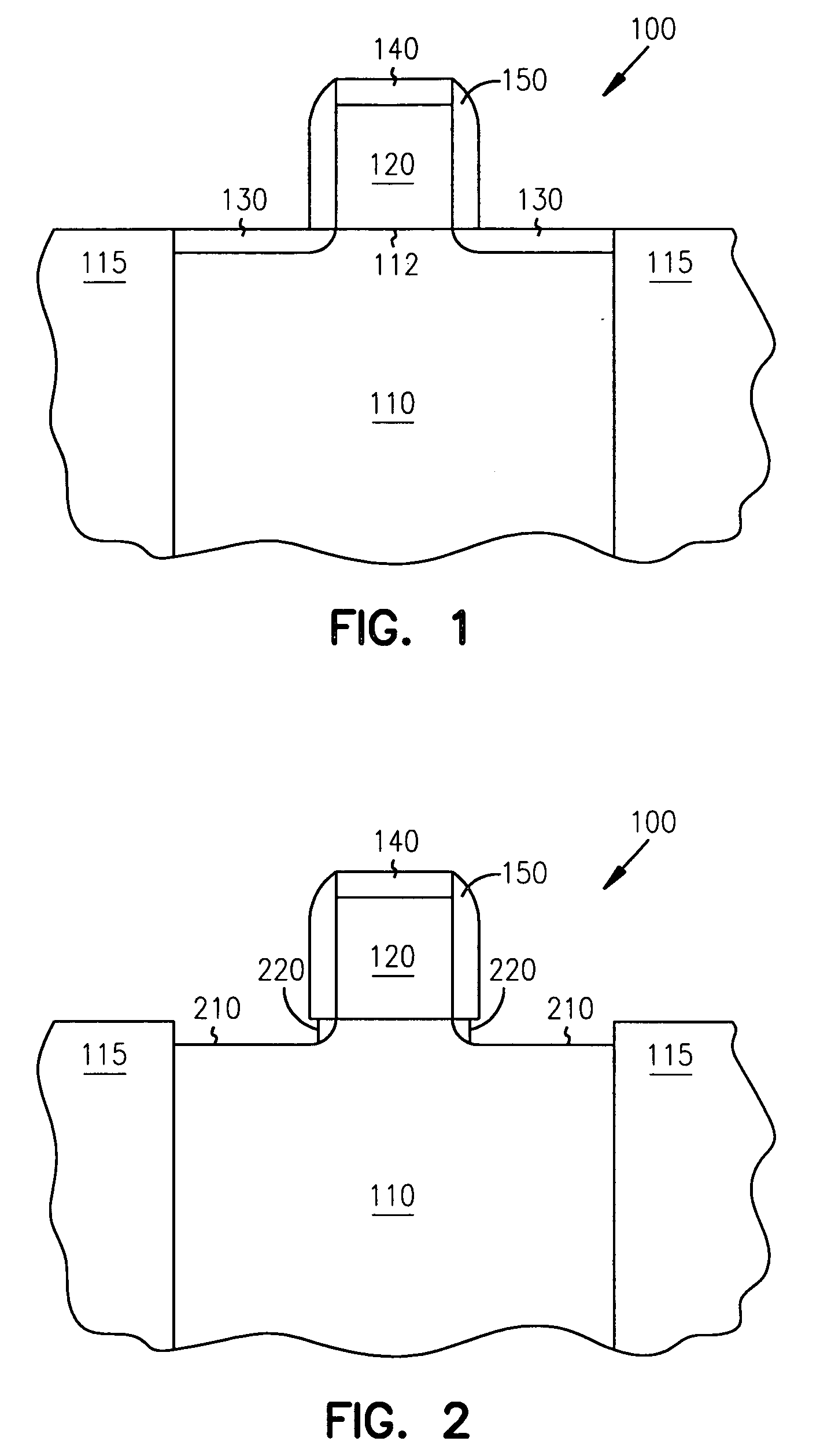
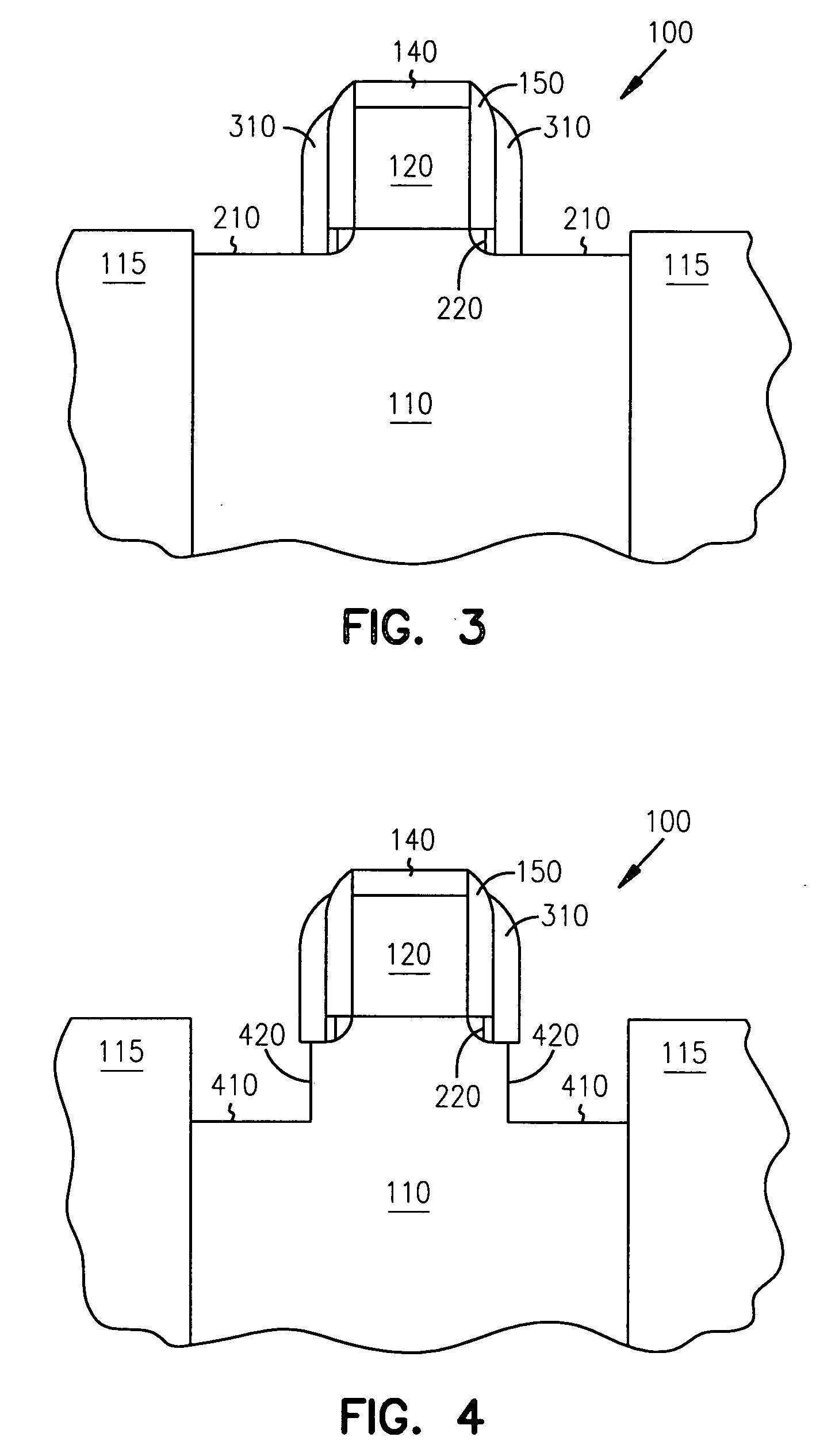
The invention provides a technique to fabricate a dielectric plug in a MOSFET. The invention includes apparatus and systems that include one or more devices including a MOSFET having a dielectric plug. The dielectric plug is fabricated by forming an oxide layer over exposed source and drain regions in the substrate including a gate electrode stack. The formed oxide layer in the source and drain regions are then substantially removed to expose the substrate in the source and drain regions and to leave a portion of the oxide layer under the gate electrode stack to form the dielectric plug and a channel region between the source and drain regions.

Description

[0001] This application is a Continuation of U.S. application Ser. No. 10 / 931,507, filed Sep. 1, 2004, which is a Divisional of U.S. application Ser. No. 10 / 175,774, filed Jun. 20, 2002, now issued as U.S. Pat. No. 6,812,103 B2, both of which are incorporated herein by reference.FIELD OF THE INVENTION [0002] The present invention relates to fabrication of integrated circuits and, in particular, to fabrication of submicron MOS devices. BACKGROUND OF THE INVENTION [0003] The structure and the various components, or features, of a metal oxide semiconductor (MOS) device such as a Field Effect Transistor (MOSFET) are generally well known. Such devices are generally formed having a source region and a drain region, of similar conductivity type, separated by a channel region, of a differing conductivity type, capped with a conductive gate. The gate to source voltage controls the passage of current through the channel region between the source and the drain regions. In a typical n-channel o...

Claims


Application Information

Patent Timeline
Patent Type & Authority Applications(United States)
IPC IPC(8): H01L29/76H01L21/336H01L29/06
CPCH01L29/0649H01L29/0653H01L29/66628H01L29/66636
Inventor WANG, HONGMEIWANG, ZHONGZE
Owner MICRON TECH INC
Learn More