Semiconductor device and method for manufacturing the same

a semiconductor and device technology, applied in semiconductor devices, capacitors, electrical devices, etc., can solve the problems of large non-uniformity in polishing speed, scratches, etc., to achieve the effect of reducing global step difference, accelerating step leveling, and suppressing peeling of lower electrodes and scratches

Inactive Publication Date: 2006-03-23
PANNOVA SEMIC
View PDF3 Cites 2 Cited by
  • Summary
  • Abstract
  • Description
  • Claims
  • Application Information

AI Technical Summary

Benefits of technology

[0023] It is an object of the present invention to present a method for manufacturing a semiconductor device, with which leveling of steps is accelerated when polishing an insulating film that buries the lower electrodes of capacitor elements, with which insufficient polishing of the burying insulating film, peeling of the lower electrodes and scratches are suppressed, and with which the global step difference can be reduced.

Problems solved by technology

This peeled metal wiring 7 may become a cause for scratches, resulting in a chain of peeling of metal wiring 7 and occurrence of scratches.
This becomes a cause for peeling of the lower electrodes 6.
As explained above, when memory cell array portions with different array surface area and peripheral circuit portions are both present, then there are regions at which the leveling of steps is accelerated and other regions that are polished at the polishing speed of the solid film, and when looking at the entire wafer surface, the non-uniformities in the polishing speed are large.
As a result, the global step difference is large, and it is difficult to eliminate insufficient polishing and avoid scratches both.
Such insufficient polishing, peeling of the lower electrodes and scratches cause bit defects in the ferroelectric memory and lower the production yields.
Moreover, in ferroelectric memories, the global step difference between the memory cell array portion and other portions (for example peripheral logic circuitry in system LSI with integrated FeRAM) may lead to an insufficient DOF (depth of focus) of lithography in the wiring step, and may result in shorts between conductors or variations in the wiring resistance, and may directly affect the production yield.

Method used


Image

  • Semiconductor device and method for manufacturing the same
  • Semiconductor device and method for manufacturing the same
  • Semiconductor device and method for manufacturing the same

Examples


embodiment 1

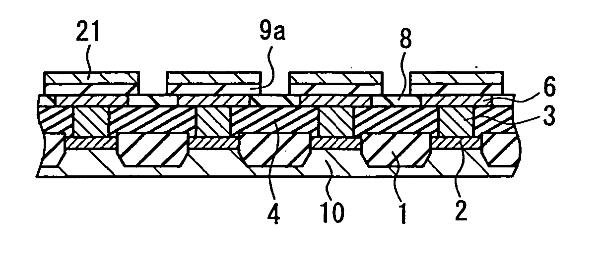
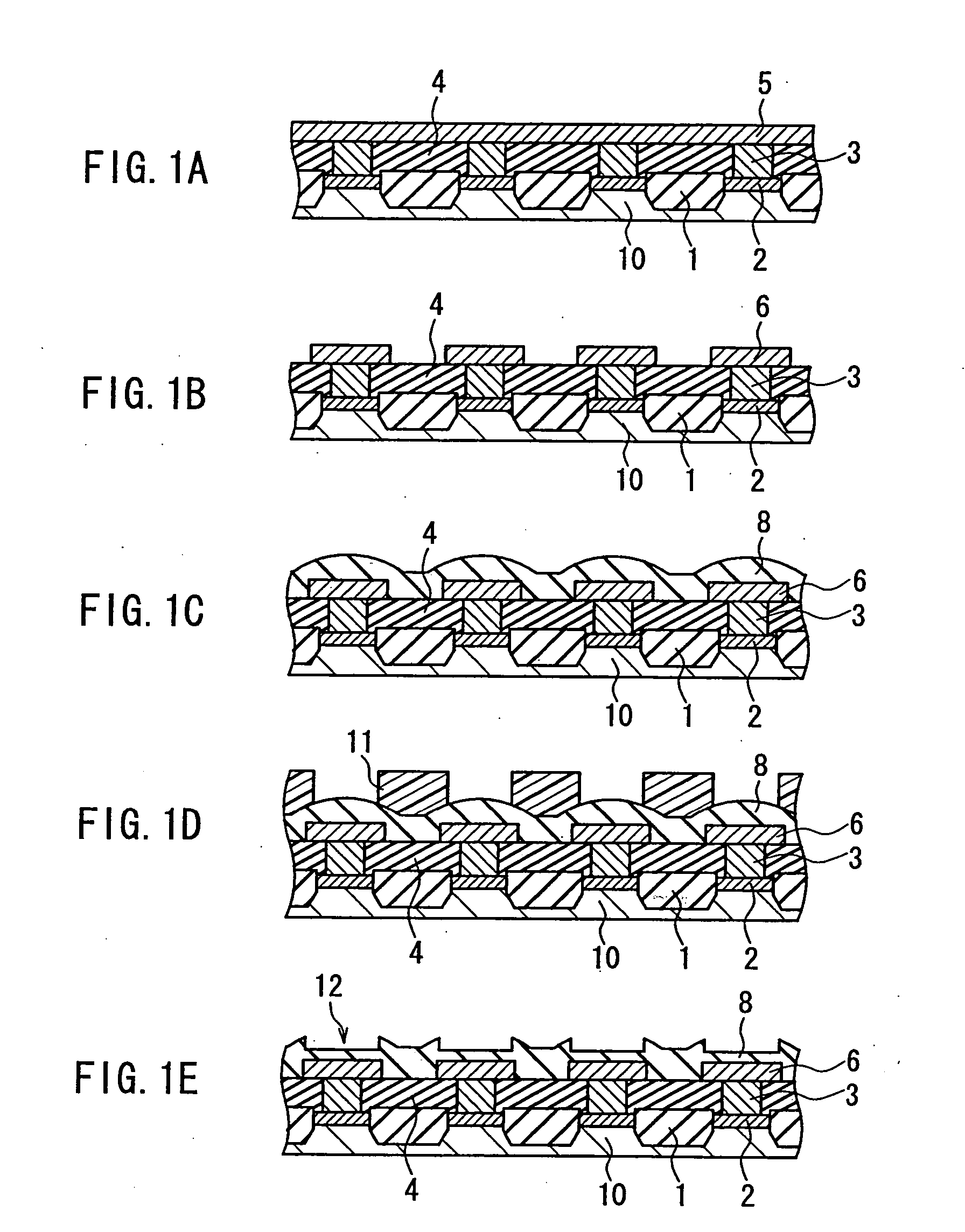
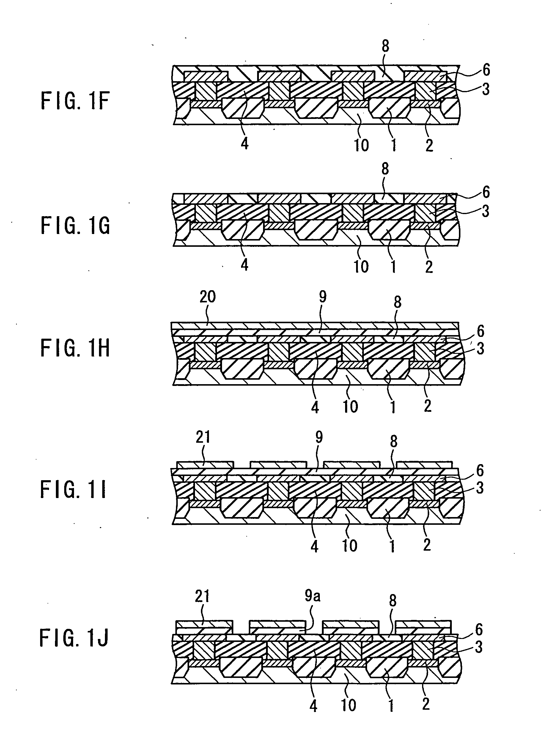
[0052] A method for manufacturing a ferroelectric memory in accordance with Embodiment 1 of the present invention is described with reference to FIGS. 1A to 1J. These drawings show a section of a memory cell array portion during the steps of manufacturing a ferroelectric memory.

[0053] First, as shown in FIG. 1A, isolation regions 1 are formed on a semiconductor substrate 10, and a high-concentration impurity diffusion layer 2 is formed between the isolation regions 1. Then, an interlayer insulation film 4 made of SiO2 is formed on the isolation regions 1 and the impurity diffusion layer 2, and contact plugs 3 (made of tungsten) that are electrically connected to the impurity diffusion layers 2 are formed in the interlayer insulation film 4. A layered film (of 300 nm thickness) including a titanium nitride barrier layer (150 nm thick) and a platinum film (150 nm thick) serving as a first conductive film 5 is formed on the interlayer insulation film 4 and the contact plugs 3.

[0054] ...

embodiment 2

[0067] The following is a description of a method for manufacturing a ferroelectric memory according to Embodiment 2 of the present invention, with reference to FIGS. 2A to 2F. FIGS. 2A to 2F shows a section of a memory cell array portion during the steps of manufacturing a ferroelectric memory. This embodiment is an example of a modification of the manufacturing method according to Embodiment 1. The steps in FIGS. 2A to 2D are similar to those in FIGS. 1A to 1D, so that their further explanation has been omitted.

[0068] As shown in FIG. 2E, the insulating film 8 at the aperture portions of the resist pattern 11 is partially removed by dry etching to form the recesses 12. It is preferable that the depth of the recesses 12 is as deep as possible. By forming the recesses 12, the polishing amount of the insulating film 8 in the following polishing step can be reduced, accelerating the step leveling.

[0069] Then, as shown in FIG. 2F, the insulating film 8 is polished by CMP to planarize...

embodiment 3

[0072] Referring to FIGS. 3Aa to 3Af, the following is a description of a method for manufacturing a ferroelectric memory according to Embodiment 3 of the present invention. FIGS. 3Aa to 3Af show sectional views of a memory cell array portion during the steps of manufacturing a ferroelectric memory. FIGS. 3Ba to 3Bf show sectional views of a metal wiring portion. The steps of FIGS. 3Aa to 3Af correspond to the steps of 3Ba to 3Bf, and are performed at the same time.

[0073] First, in a memory cell array portion, isolation regions 1 are formed on a semiconductor substrate 10, and a high-concentration impurity diffusion layer 2 is formed between the isolation regions 1, as shown in FIG. 3Aa. Then, an interlayer insulation film 4 made of SiO2 is formed on the isolation regions 1 and the impurity diffusion layer 2, and contact plugs 3 (made of tungsten) that are electrically connected to the impurity diffusion layers 2 are formed in the interlayer insulation film 4. A layered film (of 30...


PUM


Abstract

A method for manufacturing a semiconductor device includes the steps of forming a conductive layer over a first insulating layer formed on a substrate, and over a plurality of contact plugs formed in the first insulating layer; forming a plurality of capacitor element lower electrodes by patterning the conductive layer; forming a second insulating layer on the first insulating layer and the capacitor element lower electrodes; forming recesses in the second insulating layer at a region above the capacitor element lower electrodes; planarizing the second insulating layer by polishing; exposing the capacitor element lower electrodes; and forming a capacitive insulating film and capacitor element upper electrodes above the capacitor element lower electrodes. In polishing the second insulating layer, leveling of steps can be accelerated, insufficient polishing, peeling of the lower electrodes and generation of scratches can be suppressed, and the global step difference can be reduced.

Description

[0001] This application is a divisional of application Ser. No. 10 / 642,955, filed Aug. 18, 2003, which application is incorporated herein by reference.FIELD OF THE INVENTION [0002] The present invention relates to semiconductor devices including a capacitor element with a high dielectric material or a ferroelectric material as a capacitive insulating film, as well as to methods for manufacturing the same. BACKGROUND OF THE INVENTION [0003] The currently produced type of ferroelectric memories, which are one kind of capacitor elements, uses a so-called planar structure in which the lower electrodes are larger than the upper electrodes, and has a capacity of 1 to 64 kbit. On the other hand, the focus of current development is on ferroelectric memories with a large capacity of 256 kbit to 4 Mbit, which use a so-called stacked structure in which the lower electrodes are smaller than the upper electrodes. It is increasingly expected that these ferroelectric memories with stacked structur...

Claims


Application Information

Patent Timeline
Patent Type & Authority Applications(United States)
IPC IPC(8): H01L27/108H01L21/02H01L21/3105H01L21/8246H01L27/115
CPCH01L21/31053H01L28/60H01L27/11507H01L27/11502H10B53/30H10B53/00
Inventor MIKAWA, TAKUMIJYUUDAI, YUUJINATSUME, SHINYA
Owner PANNOVA SEMIC
Why Eureka
Try Eureka