[0062] An advantage of the invention is to provide an impedance conversion circuit, a drive circuit, and a method of controlling an impedance conversion circuit each capable of reducing the number of gray scale voltage
signal lines while maintaining the number of gray scales, and each capable of outputting gray scale voltages highly accurately.
[0063] According to one embodiment of the invention, there is provided an impedance conversion circuit for outputting a voltage corresponding to (j+k) (j is a positive integer, k is a positive integer more than 1) bits of gray scale data. The impedance conversion circuit includes: an operational
amplifier connected as a voltage follower and supplied with, as an input voltage, a voltage selected from 2j levels of voltages based on data of high j bits of the gray scale data; and an output voltage setting circuit for precharging or discharging an output of the operational amplifier based on data of a most significant bit of low k bits of the gray scale data. The operational amplifier outputs, as an output voltage, a voltage having a difference from the input voltage by a dead zone width after the output voltage setting circuit precharges or discharges the output of the operational amplifier. The dead zone width is determined by an operating current of the operational amplifier. The operating current is varied based on data of the low k bits of the gray scale data.
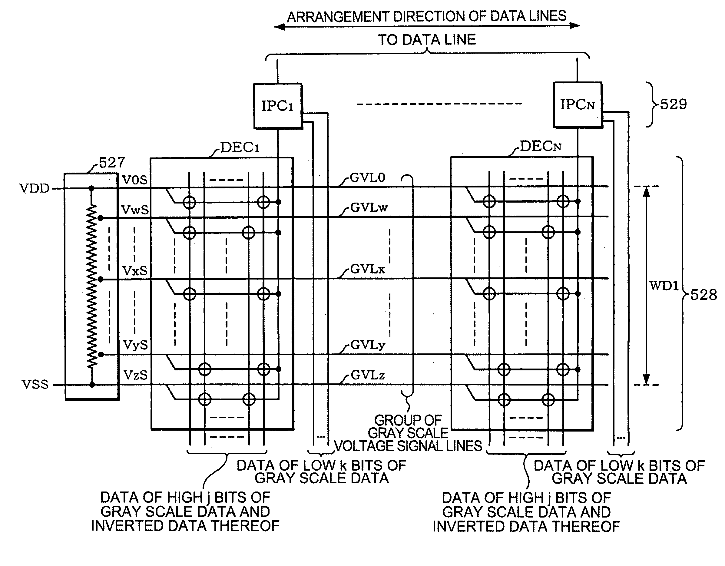
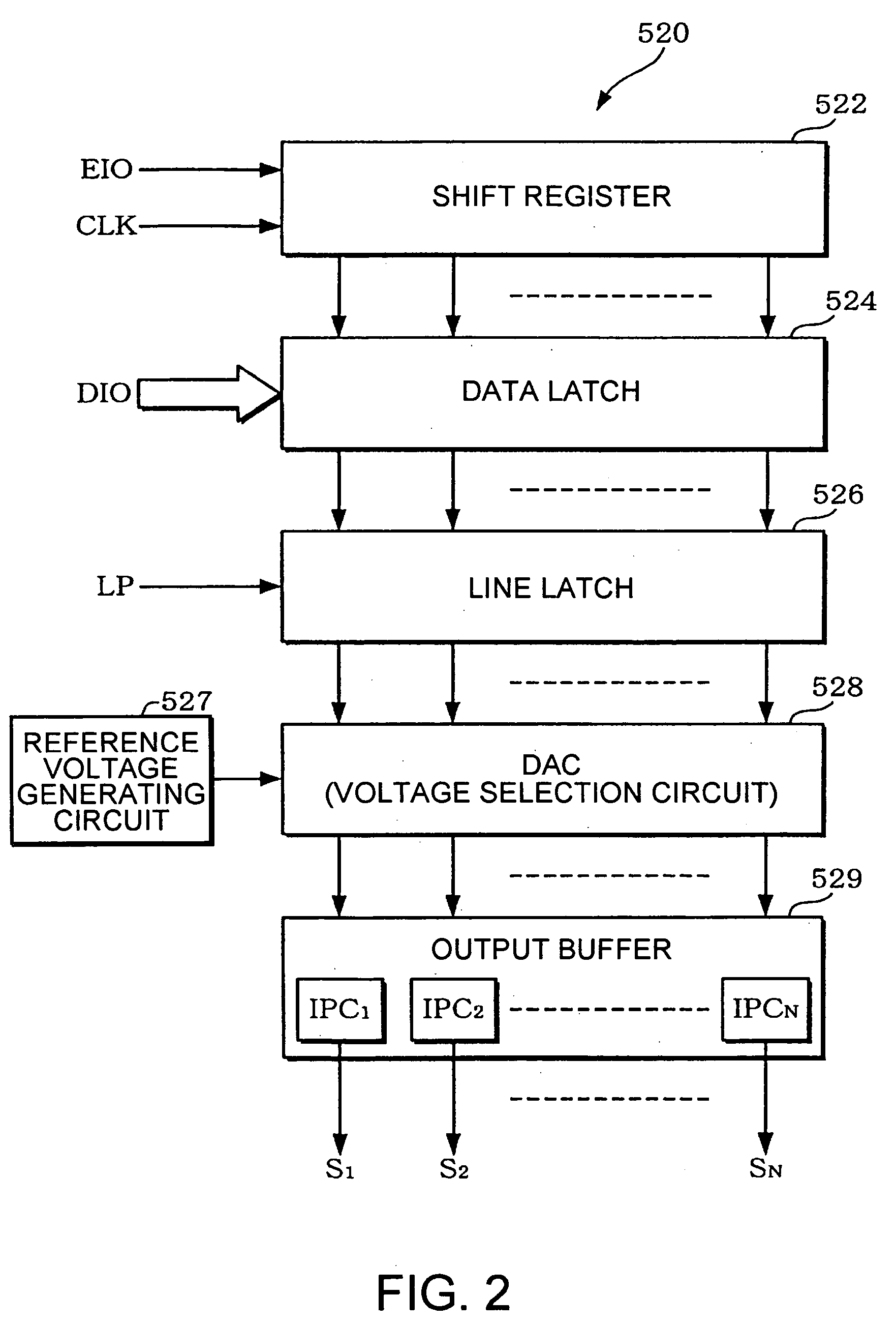
[0064] In this embodiment, any one of 2j levels of voltages corresponding to the high j bits data of (j+k) bits gray scale data is received as the input voltage, and the impedance conversion circuit outputs the voltage corresponding to low k bits of the gray scale data from the 2k levels of voltages based on the input voltage. Therefore, it is enough to select the input voltage from the 2j levels of gray scale voltages. Thus, since the number of gray scale voltage
signal lines can be reduced while maintaining the number of gray scales, the number of gray scale voltages to be generated can be reduced. Accordingly, the number of gray scale voltage
signal lines supplied with the generated gray scale voltages can be reduced, thus reducing the width of the wiring region. As a result, the ratio of area of the wiring region of the gray scale voltage
signal lines to the whole area can be suppressed. Thus, even if the number of gray scales increases, the
chip area of the data driver to which the impedance conversion circuit is applied can be reduced to achieve cost reduction.
[0065] Furthermore, in this embodiment, the dead zone width is varied by changing the operating current of the operational amplifier to generate each gray scale voltage. Thus, even if voltage differences among gray scale voltages further decrease as the number of gray scales increases, each gray scale voltage can be defined highly precisely.
[0066] In this impedance conversion circuit, the operational amplifier may include:
[0067] a first-
conductivity-type
differential amplification circuit having a first differential
transistor pair of a first
conductivity type and a first
current mirror circuit, the first differential
transistor pair having a first input-side
transistor and a first output-side transistor, a source of each of the first input-side and first output-side transistors being supplied with a current from a first
current source, a gate of the first input-side transistor being supplied with the input voltage, a gate of the first output-side transistor being supplied with the output voltage, and the first
current mirror circuit generating a
drain current of each of the first input-side and first output-side transistors; a second-
conductivity-type
differential amplification circuit having a second differential transistor pair of a second conductivity type and a second
current mirror circuit, the second differential transistor pair having a second input-side transistor and a second output-side transistor, a source of each of the second input-side and second output-side transistors being supplied with a current from a second
current source, a gate of the second input-side transistor being supplied with the input voltage, a gate of the second output-side transistor being supplied with the output voltage, and the second current mirror circuit generating a
drain current of each of the second input-side and second output-side transistors; and an output circuit having a first drive transistor of the second conductivity type and a second drive transistor of the first conductivity type, a
gate voltage of the first drive transistor being controlled based on a drain voltage of the first input-side transistor of the first differential transistor pair, a
gate voltage of the second drive transistor being controlled based on a drain voltage of the second input-side transistor of the second differential transistor pair, drains of the first and second drive transistors being coupled to each other, and the output circuit outputting, as the output voltage, a voltage at a
coupling node of the drains. A first input-side current driving capability of the first input-side transistor may be lower than a first output-side current driving capability of the first output-side transistor. A second input-side current driving capability of the second input-side transistor may be lower than a second output-side current driving capability of the second output-side transistor. A current of at least one of the first and second current sources may be controlled based on the data of the low k bits of the gray scale data to vary the dead zone width.


