Light emitting diode device
a technology of light-emitting diodes and diodes, which is applied in the direction of organic semiconductor devices, electroluminescent light sources, electric lighting sources, etc., can solve the problems of interference, interference becomes prominent, and the luminous efficiency may be degraded, so as to eliminate the interference
- Summary
- Abstract
- Description
- Claims
- Application Information
AI Technical Summary
Benefits of technology
Problems solved by technology
Method used
Image

Examples
examples
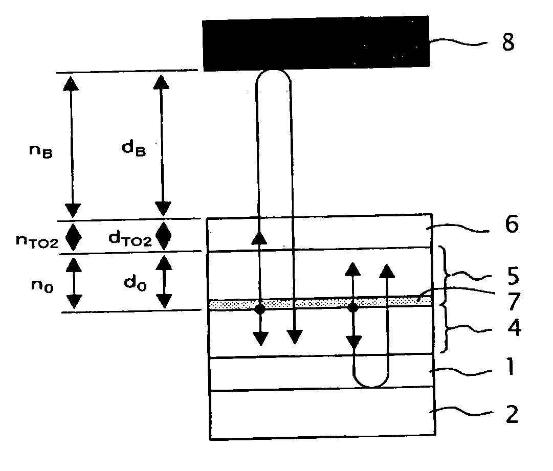
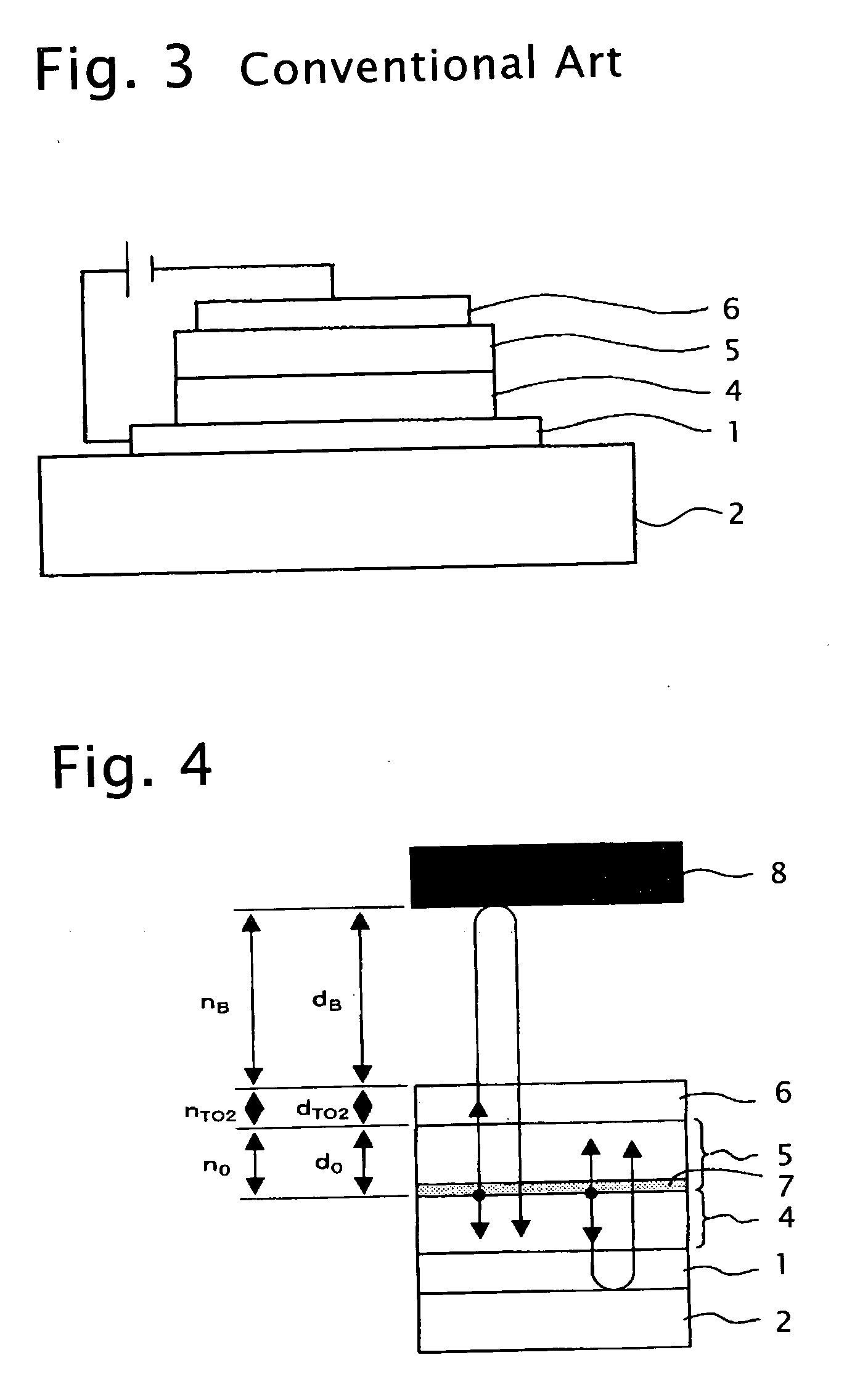
[0147] Next, Examples 1 to 13 concerning the OLED device of the invention and Comparative Examples 1 to 5 will be described. First, in Examples 1 to 12 the structure of the OLED device according to the embodiment of the invention shown in FIG. 4 was used as a basic structure. Accordingly, the common constituents in the structures of Examples 1 to 9 will be described below.
examples 1 to 9
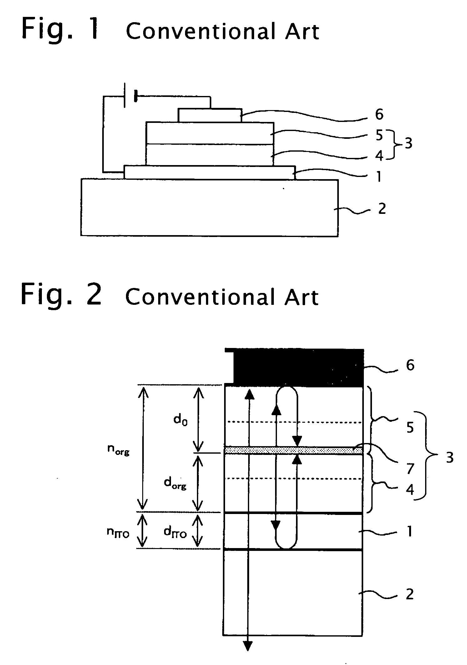
[0148] An ITO transparent electrode constituting the first transparent electrode layer (the anode) 1 was formed on a glass substrate constituting the transparent substrate 2 by the sputtering method. Sheet resistance of ITO was set to 10 ohm / sq. Then, the ITO transparent electrode 1 was etched into a given shape, and was subjected to ultrasonic cleaning by use of acetone, isopropyl alcohol, and / or the like. Thereafter, the ITO transparent electrode 1 was dried. Moreover, the glass substrate 2 was further subjected to UV-O3 cleaning, and was set in a vacuum deposition chamber. The pressure inside the chamber was reduced to about 1×10⁻⁵ Torr, and the hole transport layer 4 was formed on the ITO transparent electrode 1 in the film thickness of 100 nm. Subsequently, the organic light emitting layer 5 with addition of a blue light-emitting material configured to emit light having an emission spectrum shown in FIG. 8 (such a material will be hereinafter referred to as a “blue light-emitti...
example 10
[0150] In Example 10, the configuration ranging from the glass substrate 2 to the IZO transparent electrode 6 was similar to Examples 1 to 9 described above, whereas an oil layer in the film thickness of about 0.5 mm was formed on the IZO transparent electrode 6 instead of the first buffered layer and the reflecting mirror 8. The refractive index of the oil layer was set to 1.55 relative to the light having the wavelength of 450 nm.
PUM
 Abstract
Description
Claims
Application Information
 - R&D
- Intellectual Property
- Life Sciences
- Materials
- Tech Scout
- Unparalleled Data Quality
- Higher Quality Content
- 60% Fewer Hallucinations
Browse by: Latest US Patents, China's latest patents, Technical Efficacy Thesaurus, Application Domain, Technology Topic, Popular Technical Reports.
© 2025 PatSnap. All rights reserved.Legal|Privacy policy|Modern Slavery Act Transparency Statement|Sitemap|About US| Contact US: help@patsnap.com