
Semiconductor integrated circuit device

a technology of integrated circuits and semiconductors, applied in the direction of semiconductor devices, basic electric elements, electrical appliances, etc., can solve problems such as device failure, charge traps, and the characteristic of memory cell transistors may be deteriorated

Active Publication Date: 2006-02-23
KIOXIA CORP
View PDF13 Cites 49 Cited by
  • Summary
  • Abstract
  • Description
  • Claims
  • Application Information

AI Technical Summary

Benefits of technology

[0031] a third insulating film which is formed between the gate electrodes of the first cell unit and between the gate electrodes of the second cell unit on the first cell unit, second cell unit and diffusion layers with the first and second insulating films disp...

Problems solved by technology

This is caused by misalignment of the photomask.
As a result, a leak current increases to make the device faulty.
However, the silicon nitride film used as the barrier insulating film contains a large amount of hydrogen and tends to cause charge traps.
Therefore, the characteristic of a memory cell transistor may be deteriorated in some cases by an influence of charges, for example, electrons trapped in portions of the silicon nitride film which are formed on the diffusion layers formed in the semiconductor substrate between the gate electrodes and the gate electrode side walls.
When the parasitic capacitance between the floating gates becomes large, a variation in the threshold voltage of a memory cell transistor caused by an influence by a variation in the amount of charges stored in the adjacent floating gate becomes large, thereby making it difficult to control the threshold voltage.
Further, when the parasitic capacitance between the control gates becomes large, the wiring delay caused when the control gate is driven becomes large, thereby making the operation speed low.
However, in this case, it is necessary to perform the silicon oxide film forming process at high temperatures for a long period of time.
As a result, the manufacturing cost will rise and miniaturization of elements becomes difficult.

Method used


Image

  • Semiconductor integrated circuit device
  • Semiconductor integrated circuit device
  • Semiconductor integrated circuit device

Examples


first embodiment

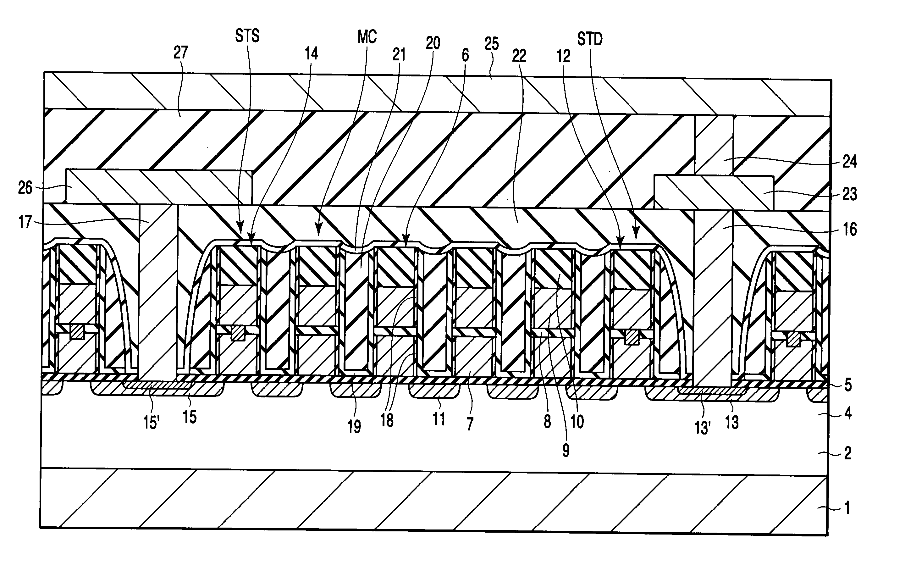
[0085] The first embodiment of this invention is explained with reference to FIGS. 1 to 9 by taking a NAND type nonvolatile semiconductor memory device as an example.

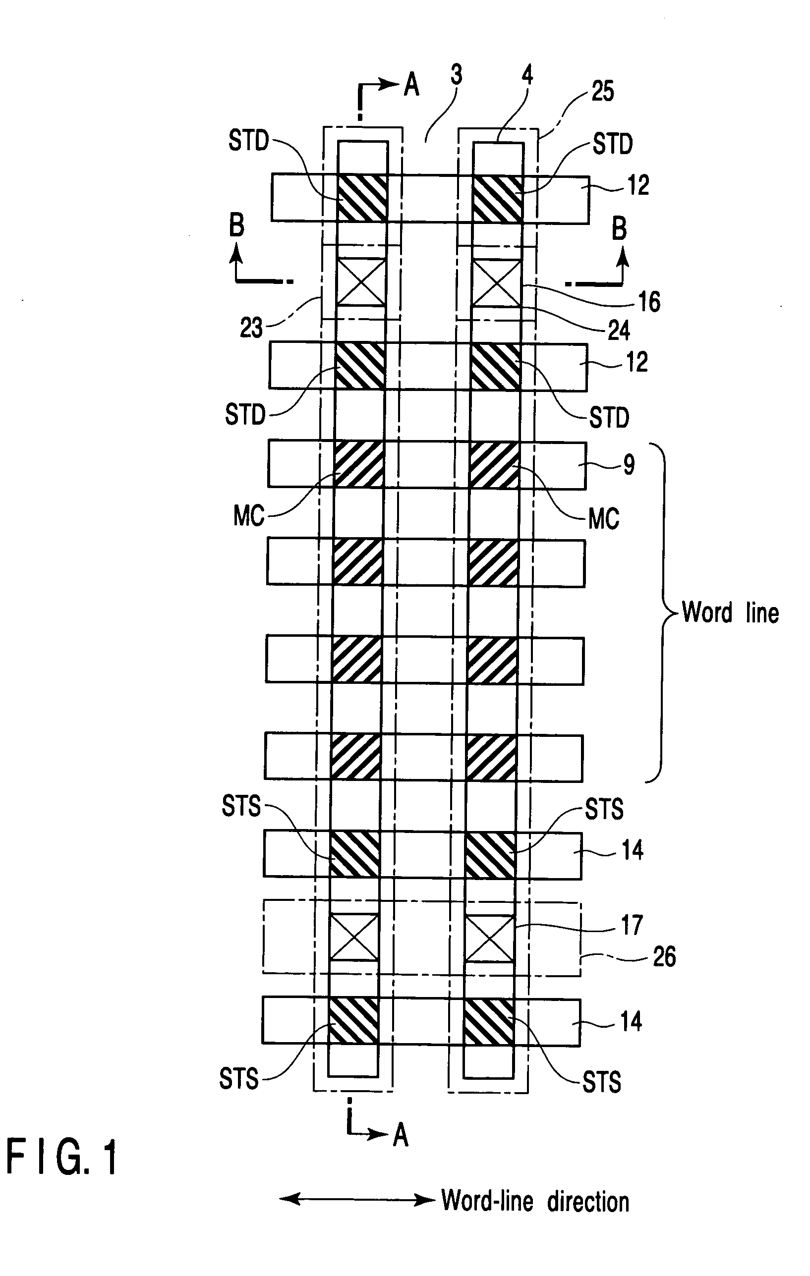
[0086]FIG. 1 is a plan view showing an example of the plane pattern of a NAND type nonvolatile semiconductor memory device according to the first embodiment of this invention.

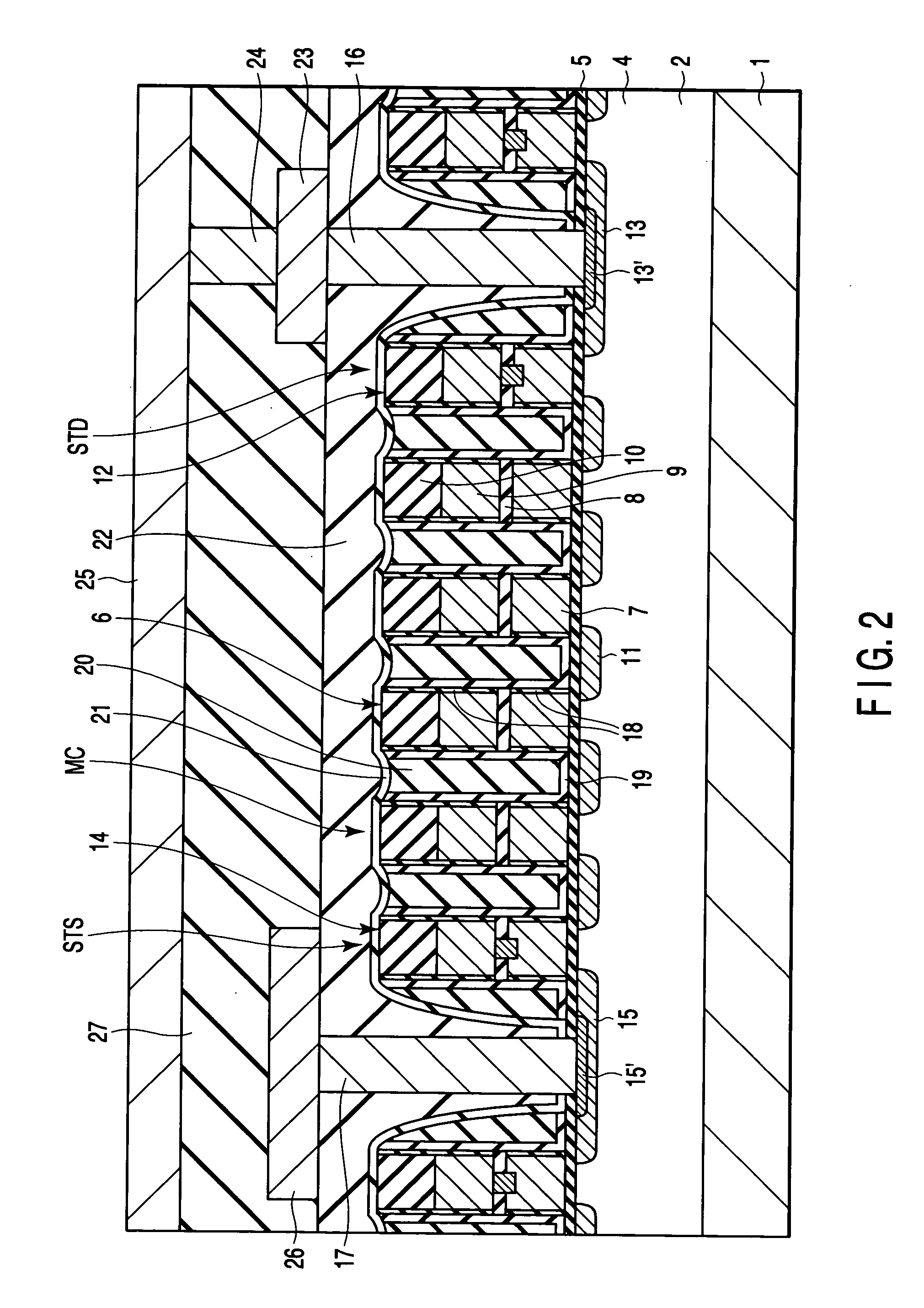
[0087] As shown in FIG. 1, each NAND cell unit has four series-connected memory cells MC connected between a drain-side selection transistor STD and a source-side selection transistor STS on a corresponding one of element regions 4 which are divided by an element isolation region 3. The memory cells MC arranged in a word line direction or in a horizontal direction in the drawing are connected to a corresponding one of common control gate lines (word lines) 9. The drain-side selection transistors STD arranged in the word line direction are connected to a corresponding one of common drain-side selection gate lines 12 and the source-side selection t...

second embodiment

[0164] The second embodiment is explained with reference to FIG. 11. The plane pattern of a nonvolatile semiconductor memory device according to the second embodiment is the same as that of the first embodiment. The plan view thereof corresponds to FIG. 1.

[0165]FIG. 11 is a cross sectional view taken along the A-A line of FIG. 1.

[0166] The second embodiment is different from the first embodiment in that a third insulating film 21 is filled to the height of a control gate electrode 9. The other portions are the same as those of the first embodiment, and therefore, the explanation thereof is omitted.

[0167] As shown in FIG. 11, in the second embodiment, the third insulating film 21 is filled in each concave portion between memory cell gate electrodes 6 which is caused by forming a second insulating film 20 thinner than that of the first embodiment. At this time, the lowest portion of the filled third insulating film 21 is set higher than the highest portion of a floating gate electr...

third embodiment

[0169] The third embodiment is explained with reference to FIG. 12. The plane pattern of a nonvolatile semiconductor memory device according to the third embodiment is the same as that of the first embodiment. The plan view thereof corresponds to FIG. 1.

[0170]FIG. 12 is a cross sectional view taken along the A-A line of FIG. 1.

[0171] The third embodiment is different from the first embodiment in that a first insulating film 19 and second insulating film 20 are not etched out from the upper surface of a bit line contact diffusion layer 13 and source line contact diffusion layer 15. The other portions are the same as those of the first embodiment, and therefore, the explanation thereof is omitted.

[0172] As shown in FIG. 12, in the third embodiment, a third insulating film 21 is deposited after the first insulating film 19 and second insulating film 20 are deposited.

[0173] Like the first and second embodiments, the first insulating film 19 and second insulating film 20 are left beh...


PUM


Abstract

A semiconductor integrated circuit device includes first, second gate electrodes, first, second diffusion layers, contact electrodes electrically connected to the first diffusion layers, a first insulating film which has concave portions between the first and second gate electrodes and does not contain nitrogen as a main component, a second insulating film which is formed on the first insulating film and does not contain nitrogen as a main component, and a third insulating film formed on the first diffusion layers, first gate electrodes, second diffusion layers and second gate electrodes with the second insulating film disposed therebetween in a partial region. The second insulating film is formed to fill the concave portions and a portion between the first and second gate electrodes has a multi-layered structure containing at least the first and second insulating films.

Description

CROSS-REFERENCE TO RELATED APPLICATIONS [0001] This application is based upon and claims the benefit of priority from prior Japanese Patent Application No. 2004-242558, filed Aug. 23, 2004, the entire contents of which are incorporated herein by reference. BACKGROUND OF THE INVENTION [0002] 1. Field of the Invention [0003] This invention relates to a semiconductor integrated circuit device and more particularly to a semiconductor integrated circuit device containing a nonvolatile semiconductor memory device. [0004] 2. Description of the Related Art [0005] For example, a NAND type nonvolatile semiconductor memory device is known as a nonvolatile semiconductor memory device having two-layered gate electrodes of floating gates and control gates. [0006] The NAND type nonvolatile semiconductor memory device has a memory cell array in which a drain-side selection transistor STD and source-side selection transistor STS are arranged on both ends of a series connected circuit of memory cell ...

Claims


Application Information

Patent Timeline
IPC IPC(8): H01L29/76
CPCH01L27/11521H01L27/115H10B69/00H10B41/30H10B99/00
Inventor YAEGASHI, TOSHITAKEOZAWA, YOSHIO
Owner KIOXIA CORP
Learn More