Microwave-monolithic-integrated-circuit-mounted substrate, transmitter device for transmission only and transceiver device for transmission/reception in microwave-band communication

a monolithic integrated circuit and substrate technology, applied in the direction of printed circuit components, printed circuit non-printed electric components association, printed circuit incorporation, etc., can solve the problems of not being able to achieve simple mmic, unable to apply mmic in advance to the substrate and mount components, and unable to simultaneously complete soldering. , to achieve the effect of efficient heat dissipation

Inactive Publication Date: 2006-02-16
SHARP KK
View PDF6 Cites 15 Cited by
  • Summary
  • Abstract
  • Description
  • Claims
  • Application Information

AI Technical Summary

Benefits of technology

[0012] An object of the present invention is to provide an MMIC-mounted substrate that requires no flanged MMIC to be prepared, can be assembled without handwork soldering and can efficiently dissipate heat.

Problems solved by technology

A problem in the aforementioned conventional techniques is that the flanged MMIC, not a simple MMIC, has to be prepared as a high power amplifier.
In this state, even if the whole is heated in a reflow bath, most of the heat is taken by metal chassis 3 and thus the soldering of good quality cannot be accomplished.
Therefore, unlike common surface-mount components, it is impossible to apply solder in advance to the substrate and mount components and simultaneously complete soldering.
This means that flanged MMIC 7 is first secured to metal chassis 3 with screws 4 and thereafter terminals 7c are soldered by handwork, possibly causing deterioration in reliability due to the handwork.

Method used


Image

  • Microwave-monolithic-integrated-circuit-mounted substrate, transmitter device for transmission only and transceiver device for transmission/reception in microwave-band communication
  • Microwave-monolithic-integrated-circuit-mounted substrate, transmitter device for transmission only and transceiver device for transmission/reception in microwave-band communication
  • Microwave-monolithic-integrated-circuit-mounted substrate, transmitter device for transmission only and transceiver device for transmission/reception in microwave-band communication

Examples


first embodiment

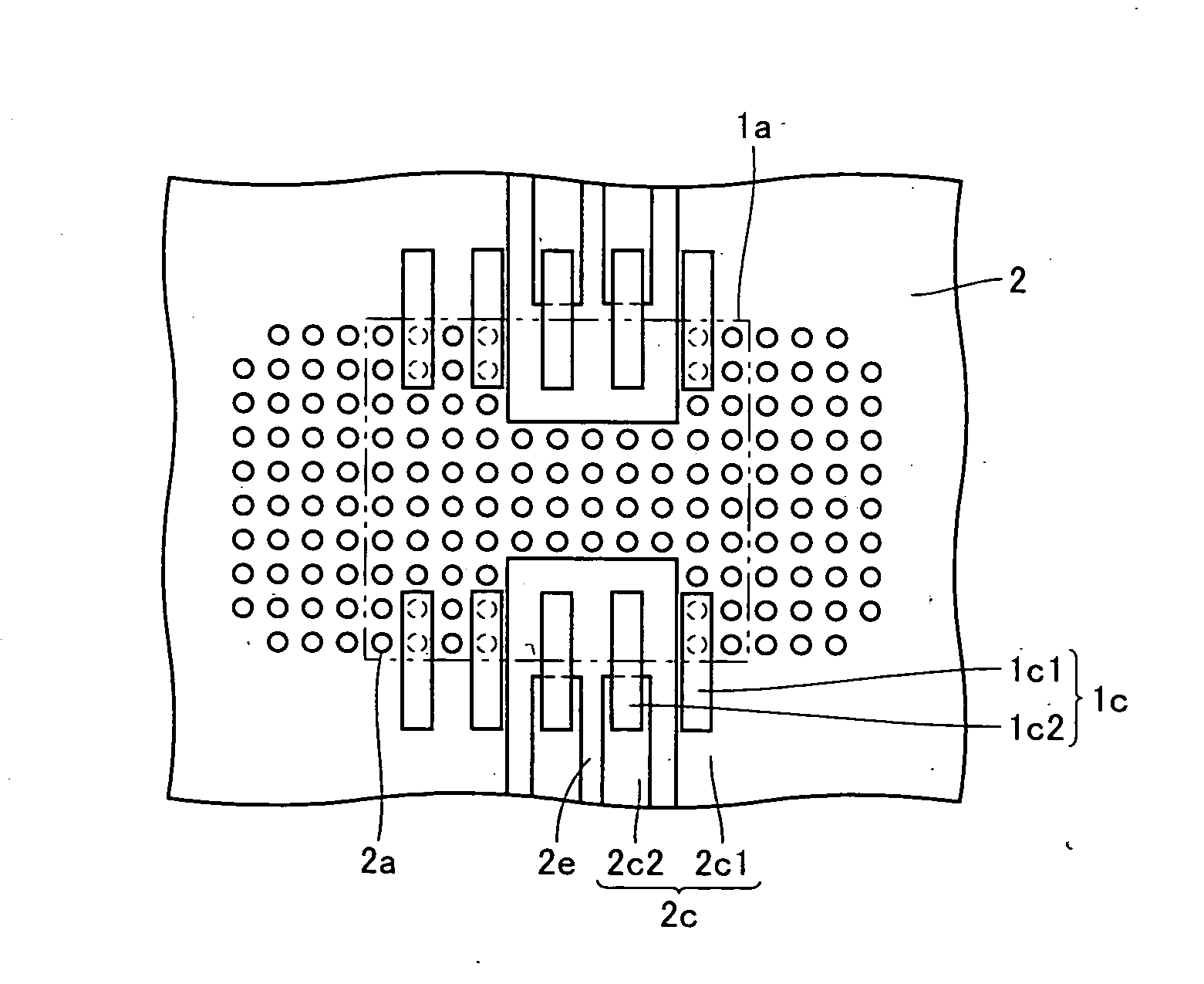
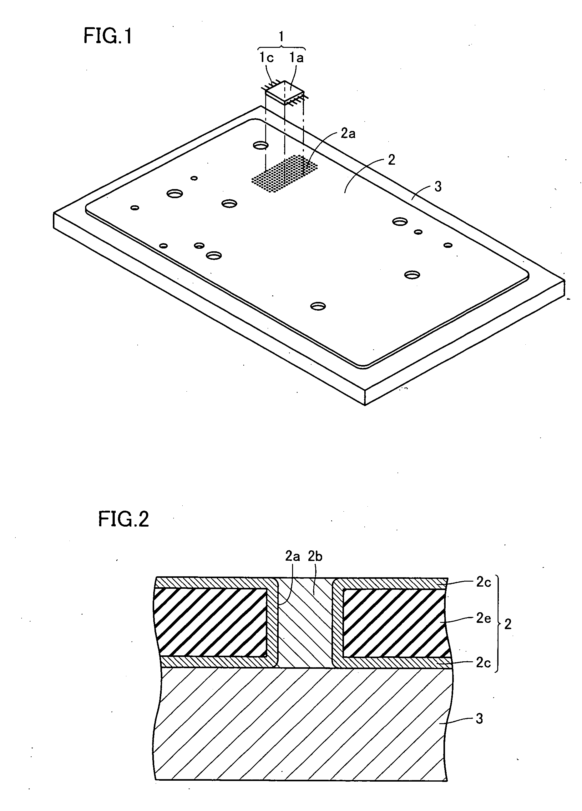
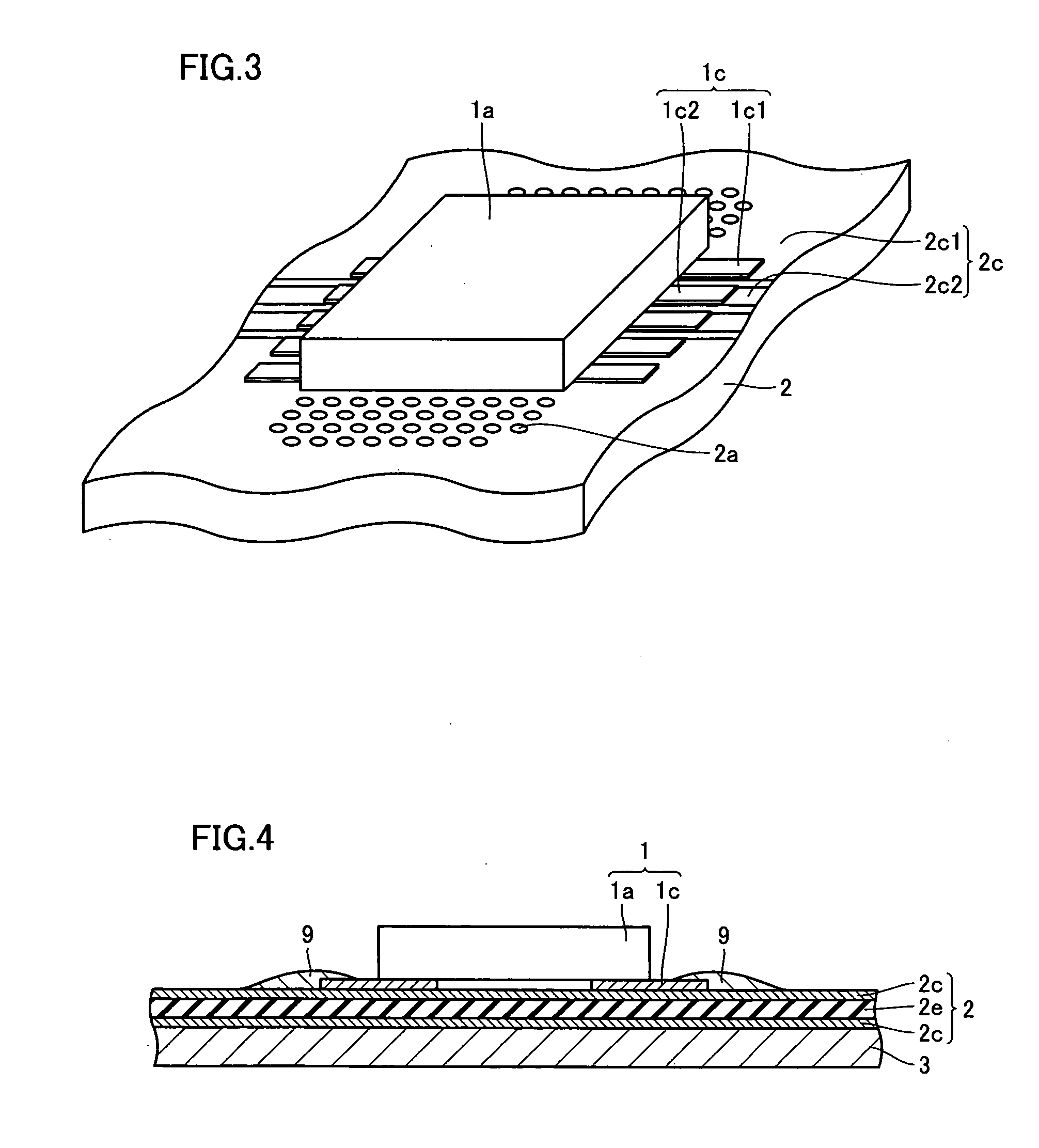
[0041] Referring to FIGS. 1 to 6, an MMIC-mounted substrate according to a first embodiment of the present invention is described. The MMIC-mounted substrate, as shown in FIG. 1, includes a double-metal-foil dielectric substrate 2, an MMIC 1 and a metal chassis 3. In FIG. 1, for the purpose of convenience of description, MMIC 1 is shown to be apart from double-metal-foil dielectric substrate 2. MMIC 1 is a surface-mount high power amplifier and is provided on one side of double-metal-foil dielectric substrate 2. To the other side of double-metal-foil dielectric substrate 2, metal chassis 3 is attached. FIG. 2 is a partial enlarged cross sectional view of the MMIC-mounted substrate shown in FIG. 1. Double-metal-foil dielectric substrate 2 has, as shown in FIG. 2, a copper foil pattern 2c as a metal foil pattern formed on both sides of a dielectric substrate 2e. Double-metal-foil dielectric substrate 2 has a region where a number of through holes 2a are arranged. MMIC 1 is mounted in ...

second embodiment

[0054] Referring to FIGS. 7 to 9, an MMIC-mounted substrate according to a second embodiment of the present invention is described. The MMIC-mounted substrate, as shown in FIG. 7, includes a double-metal-foil dielectric substrate 2, an MMIC 1, a metal chassis 3, and screws 4. In FIG. 7, for the purpose of convenience of description, MMIC 1 is shown to be apart from double-metal-foil dielectric substrate 2. Screws 4 are passed through double-metal-foil dielectric substrate 2 to be connected to metal chassis 3. FIG. 8 is a plan view before screws 4 are attached. As shown in FIG. 8, screw holes 2d are provided outside the region, occupied by an MMIC body 1a, of double-metal-foil dielectric substrate 2, and relatively close to MMIC body 1a. Screw holes 2d are provided in ground pattern 2c1.

[0055] Screw 4 is tightened in screw hole 2d as shown in FIG. 9. Screw 4 is apart from MMIC 1.

[0056] When screw 4 is tightened, screw 4 may directly be tightened and fastened to ground pattern 2c1. ...

third embodiment

[0062] Referring to FIGS. 10 and 11, an MMIC-mounted substrate according to a third embodiment of the present invention is described. The MMIC-mounted substrate includes, as shown in FIG. 10, a double-metal-foil dielectric substrate 2, an MMIC 1, a metal chassis 3, a heat dissipation plate 5, and screws 4. In FIG. 10, for the purpose of convenience of description, MMIC 1 is shown to be apart from double-metal-foil dielectric substrate 2. Heat dissipation plate 5 is in contact with the top surface of MMIC 1 and has through holes for passing screws 4 therethrough. Heat dissipation plate 5 is preferably made of metal. Screws 4 are passed through heat dissipation plate 5 and fastened while pressing heat dissipation plate 5 against MMIC 1, which is shown in the cross section of FIG. 11.

[0063] Other components and structure except those discussed above are similar to those described in connection with the first and second embodiments, and the description thereof is not repeated.

[0064] A...


PUM


Abstract

An MMIC (Microwave Monolithic Integrated Circuit)-mounted substrate includes a double-metal-foil dielectric substrate having a dielectric substrate with a metal foil pattern formed on both sides of the substrate, an MMIC that is a surface-mount high power amplifier mounted on one side of the double-metal-foil dielectric substrate, and a metal chassis attached to the other side of the double-metal-foil dielectric substrate. The double-metal-foil dielectric substrate has a plurality of through holes. A copper foil pattern that is a metal foil pattern continuously extends to cover the inner surfaces of the through holes and both sides of the dielectric substrate, and solder is buried in the through holes.

Description

[0001] This nonprovisional application is based on Japanese Patent Applications Nos. 2003-405961 and 2004-292417 filed with the Japan Patent Office on Dec. 4, 2003, and Oct. 5, 2004, respectively, the entire contents of which are hereby incorporated by reference. BACKGROUND OF THE INVENTION [0002] 1. Field of the Invention [0003] The present invention relates to a substrate having a microwave monolithic integrated circuit (hereinafter referred to as “MMIC”) mounted thereon. The MMIC-mounted substrate is chiefly used in transmission devices for satellite communication, particularly in Ku-band transceivers and Ku-band transmitters. [0004] 2. Description of the Background Art [0005] Japanese Utility Model Laying-Open No. 5-31307 discloses a conventional technique of promoting heat dissipation of a high output transistor of a high power amplifier. Further, Japanese Patent Laying-Open No. 2003-060523 discloses a conventional technique of mounting a semiconductor device, which generates a...

Claims


Application Information

Patent Timeline
Patent Type & Authority Applications(United States)
IPC IPC(8): H01L23/34H05K7/20H01L21/60H01L23/367H01L23/40H05K1/02H05K1/11H05K1/16H05K1/18H05K3/32H05K3/34
CPCH01L23/3677H01L2924/014H01L24/81H01L2224/81801H01L2924/01029H01L2924/01033H01L2924/01079H01L2924/01082H01L2924/14H01L2924/1423H01L2924/19043H05K1/0206H05K1/0243H05K3/0061H05K3/325H05K3/3421H05K2201/0715H05K2201/09572H05K2201/10409H05K2201/10689H01L2924/01005H01L2924/01006H01L23/4006
Inventor NAKAMURA, MAKIOENOKUMA, SHUNJI
Owner SHARP KK
Why Eureka
Try Eureka