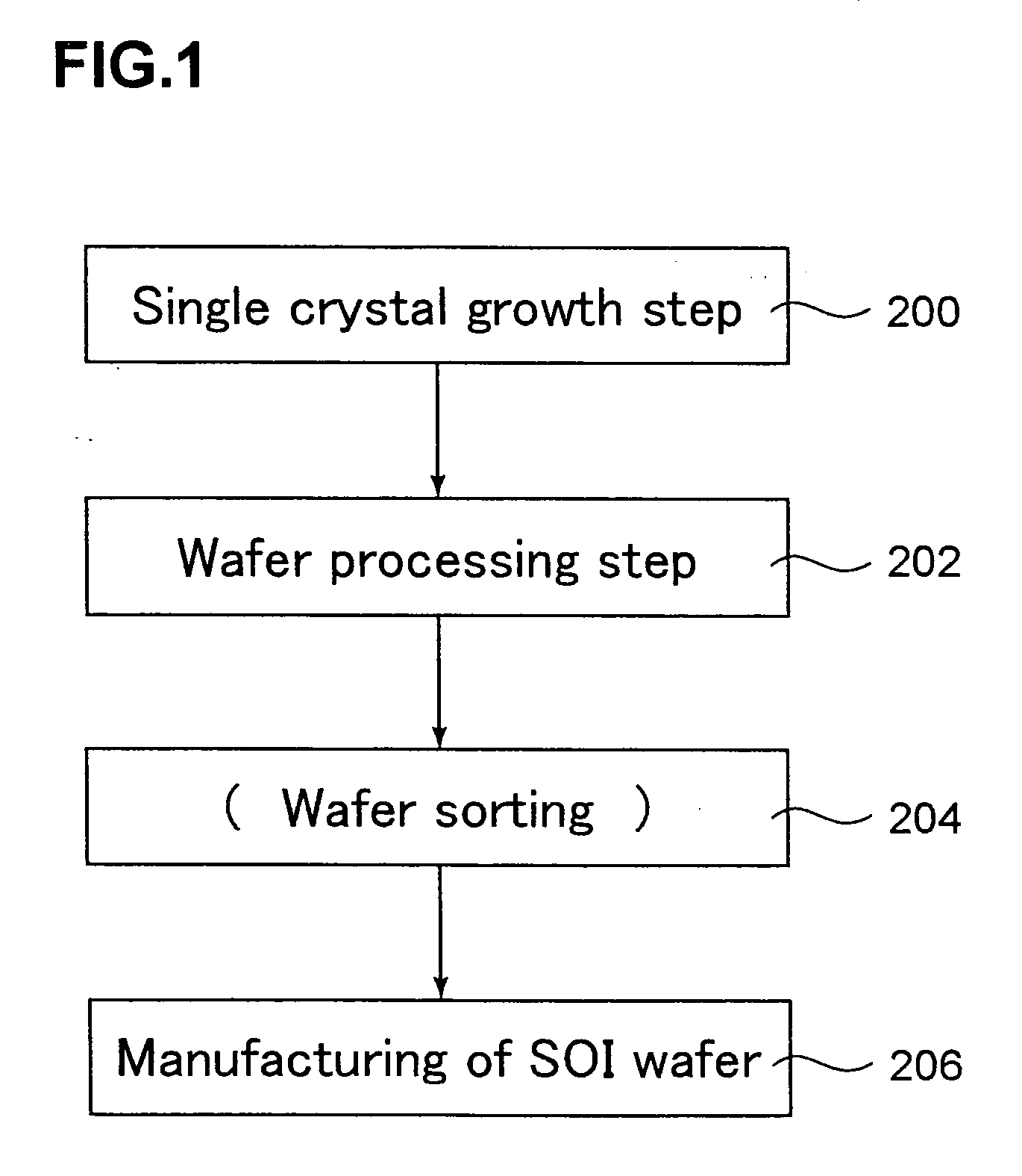
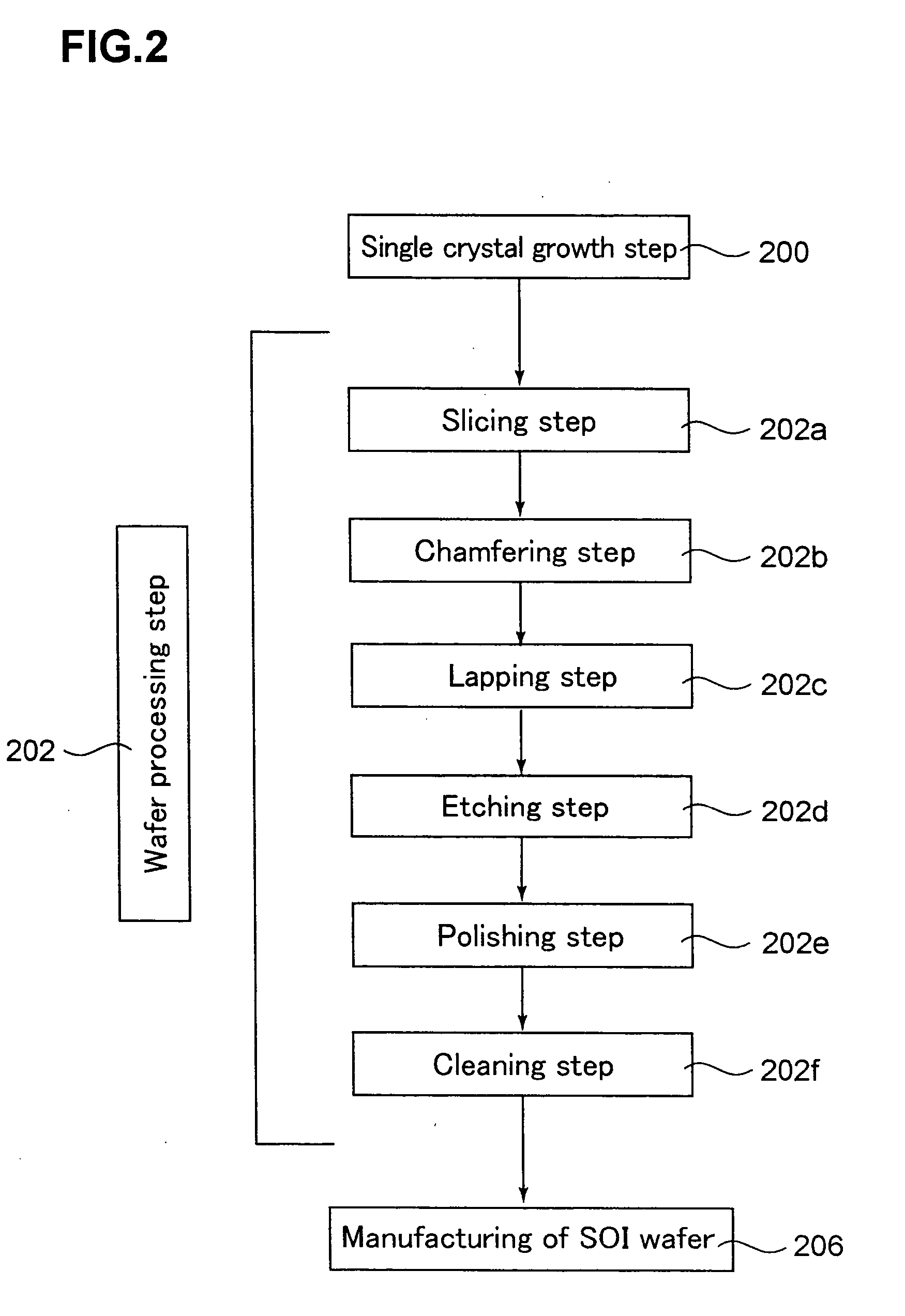
Method for manufacturing soi wafer
a technology of soi and insulator, which is applied in the direction of basic electric elements, electrical apparatus, and semiconductor devices, can solve the problems of difficult to manufacture flat wafers, and achieve the effect of reducing the generation of voids
- Summary
- Abstract
- Description
- Claims
- Application Information
AI Technical Summary
Benefits of technology
Problems solved by technology
Method used
Image


Examples
experimental example 1
[0078] At first, using, as starting wafers (base wafers and bond wafers), p-type mirror-polished silicon wafers each having a diameter of 300 mm, a orientation and a resistivity of 10 Ω·cm manufactured from an ingot grown by a CZ method, there were prepared wafers of plural levels that were mirror-polished under different wafer manufacturing conditions. The outer peripheral portions of these wafers have slightly different from each other in configuration. The peripheral configurations of the wafers of these levels were measured using a wafer configuration evaluation apparatus (Nanometro (tradename) manufactured by Kuroda Precision Industries Ltd.).
[0079] Measurement results of the configurations of the obtained wafers were compensated such that a region of between 7 mm and 10 mm away from the wafer outer periphery was set as a reference (zero) and plotted. At this time, an example of the obtained configuration profile is shown in FIG. 5.
[0080] In this experimental example, a conf...
experimental example 2
[0088] As another method for evaluating a configuration, an obtained result (a configuration profile) was subjected to a differential process to determine an inclination. SOI wafers were manufactured by the same method as that in Experimental Example 1 using, as starting wafers, wafers polished in a plurality of polishing steps, and differential profiles and generation statuses of voids were checked. As a result, a slope in a wafer where a considerably large number of voids are generated is larger than that in a wafer where a small number of voids are generated as shown in FIG. 8, for example, at a position of 5 mm away from the outer periphery. In FIG. 8, a thick line indicates a wafer where voids are easily generated, and a dotted line indicates a wafer where voids were less generated. Also, a position where an inclination is generated starts from the inside of a wafer.
[0089] In this Experimental Example, especially, slope values and generation rates of voids at a position of 5 m...
example 1
[0090] Using, as starting wafers (base wafers and bond wafers), p-type mirror-polished silicon wafers each having a diameter of 300 mm, a orientation, a resistivity of 10 Ω·cm manufactured from an ingot by a CZ method, and (TC3-10)=0.05 μm (a slope in a region of between 4.5 mm and 5.5 mm away from the outer periphery is 0.001%), SOI wafers were manufactured. A silicon oxide film of 150 nm in thickness was formed on the surface (the entire surface) of the bond wafer by thermal oxidation. Hydrogen ions were implanted into the bond wafer to form a fine air bubble layer (a sealed layer). In addition, RCA cleaning and SPM cleaning to remove organic matter were performed. Next, the oxide film on the surface of the bond wafer through which ions were implanted and the surface of the base wafer were brought into close contact with each other at room temperature.
[0091] Then, heat treatment (delaminating heat treatment) was applied thereto at 500° C. or higher to delaminate a part of the bo...
PUM
 Abstract
Description
Claims
Application Information
 - R&D
- Intellectual Property
- Life Sciences
- Materials
- Tech Scout
- Unparalleled Data Quality
- Higher Quality Content
- 60% Fewer Hallucinations
Browse by: Latest US Patents, China's latest patents, Technical Efficacy Thesaurus, Application Domain, Technology Topic, Popular Technical Reports.
© 2025 PatSnap. All rights reserved.Legal|Privacy policy|Modern Slavery Act Transparency Statement|Sitemap|About US| Contact US: help@patsnap.com