Semiconductor component, semiconductor wafer component, manufacturing method of semiconductor component, and manufacturing method of joining structure

Inactive Publication Date: 2012-06-21
PANASONIC CORP
View PDF5 Cites 0 Cited by
  • Summary
  • Abstract
  • Description
  • Claims
  • Application Information

AI Technical Summary

Benefits of technology

[0045]The present invention exhibits the effect of reducing the generation of a void in the joining layer consisting of the joining material containing Bi as an essential ingredient.

Problems solved by technology

However, when the joining material 408 is molten in the semiconductor component 401, a short circuit, a disconnection, or a change in the electrical characteristics may be caused, thereby resulting in a failure in a final product.

Method used


Image

  • Semiconductor component, semiconductor wafer component, manufacturing method of semiconductor component, and manufacturing method of joining structure
  • Semiconductor component, semiconductor wafer component, manufacturing method of semiconductor component, and manufacturing method of joining structure
  • Semiconductor component, semiconductor wafer component, manufacturing method of semiconductor component, and manufacturing method of joining structure

Examples


embodiment 1

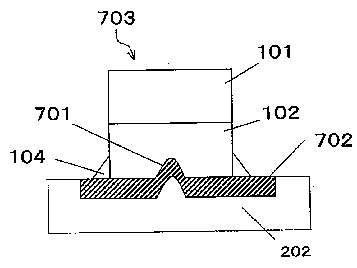
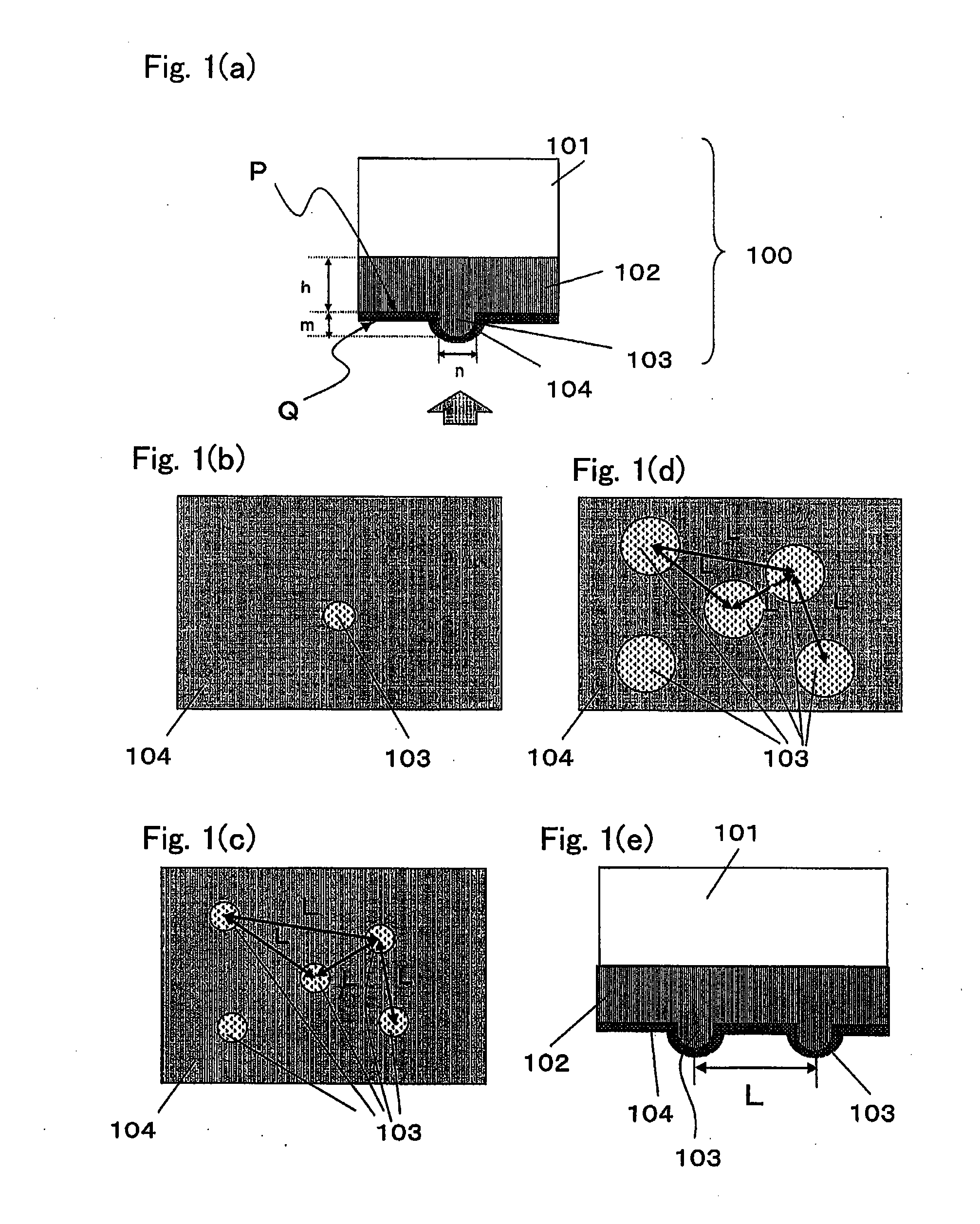
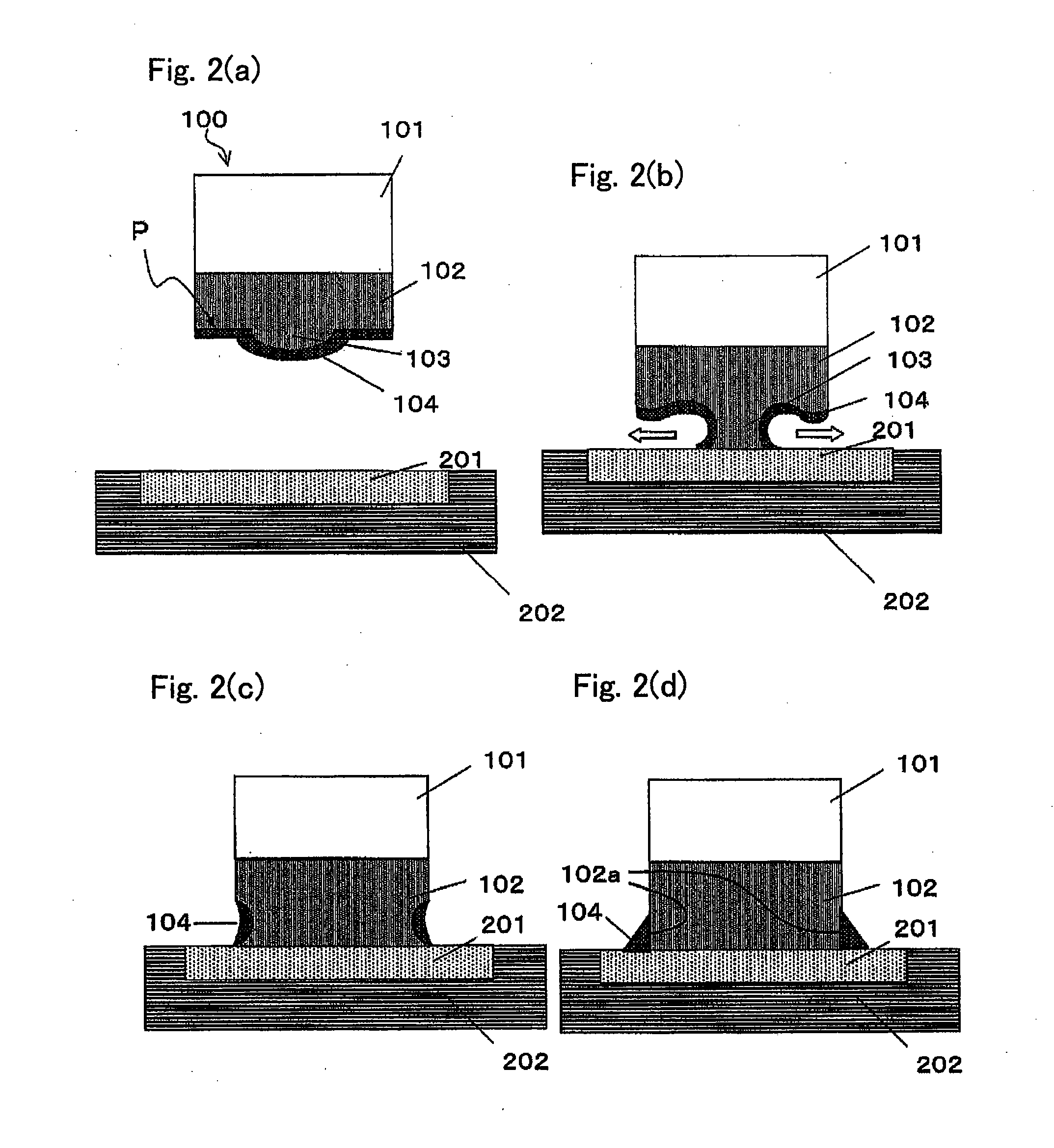
[0054]FIG. 1(a) to FIG. 1(e) are schematic diagrams of a semiconductor component according to embodiment 1 of the present invention. FIGS. 1(a) and (e) are sectional views of the semiconductor component, and FIGS. 1(b), (c) and (d) are plan views of the joining layer of the semiconductor component when viewed from the arrow direction in FIG. 1(a).

[0055]A semiconductor element 101 is made from Si, and is cut out in a size of 4.5 mm×3.55 mm from a wafer (semiconductor wafer) having a diameter of 6 inches and a thickness of 0.3 mm. The semiconductor element 101 may be made from not only Si but also Ge, and further, may also be made from a compound semiconductor, such as GaN, GaAs, InP, ZnS, ZnSe, SiC and SiGe. Further, as for the size of the semiconductor element 101, a semiconductor element having a large size of 6 mm×5 mm, or a semiconductor element 101 having a small size, such as 3 mm×2.5 mm and 2 mm×1.6 mm, may also be used according to the function of the semiconductor element 10...

embodiment 2

[0081]In the semiconductor component according to embodiment 1, the projecting section 103 is formed on the surface of the joining layer on the side opposite to the surface in contact with the semiconductor element, and is formed in a hemispherical shape whose maximum height m in the normal direction is 10 μm on the basis of the plane P (see FIG. 1(a)), and whose maximum diameter n in the plane direction is 10 μm.

[0082]However, it is also conceivable that, when the height of the projecting section is set extremely low, the air passage is easily closed. Thus, the relationship between the height of the projecting section and the presence / absence of generation of the void was verified.

[0083]FIG. 3 is a diagram showing a relationship of the void generation rate with respect to the height of the projecting section. In the experiment at this time, one projecting section was provided at the central portion of the joining layer.

[0084]The void generation rate (%) is expressed as follows:

Void...


PUM


Abstract

A semiconductor component of the present invention includes a semiconductor element and a joining layer formed on one surface of the semiconductor element and consisting of a joining material containing Bi as an essential ingredient, and projecting sections are formed on a surface of the joining layer on a side opposite to a surface in contact with the semiconductor element. By joining the semiconductor component to an electrode arranged so as to face the joining layer, the generation of a void can be suppressed.

Description

CROSS-REFERENCE TO RELATED APPLICATIONS[0001]This application is a U.S. national phase application of PCT International Patent Application No. PCT / JP2010 / 004655 filed Jul. 20, 2010, claiming the benefit of priority of Japanese Patent Application No. 2009-172709 filed Jul. 24, 2009, all of which are incorporated by reference herein in their entirety.TECHNICAL FIELD[0002]The present invention relates to a semiconductor component having, on the surface of a semiconductor element, a joining layer made from a joining material containing Bi as an essential ingredient, a semiconductor wafer component, a manufacturing method of the semiconductor component, and a manufacturing method of a joining structure.BACKGROUND ART[0003]A semiconductor component is mounted on a substrate using a soldering material. For example, as a soldering material used for joining a semiconductor component such as an IGBT (Insulated Gate Bipolar Transistor) to a substrate, a soldering material having a composition ...

Claims


Application Information

Patent Timeline
IPC IPC(8): H01L23/498H01L21/60
CPCH01L2224/32257H01L2924/1305H01L2224/73265H01L2224/83191H01L2224/838H01L2924/01004H01L2924/01005H01L2924/01015H01L2924/01029H01L2924/0103H01L2924/01032H01L2924/01047H01L2924/0105H01L2924/01057H01L2924/01074H01L2924/01078H01L2924/01082H01L2924/10329H01L2924/13055H01L24/29H01L24/32H01L24/48H01L24/83H01L2224/2901H01L2224/29113H01L2224/32245H01L2224/48091H01L2924/01006H01L2924/01019H01L2924/01033H01L2924/014H01L2224/29101H01L2924/0132H01L2924/0133H01L2924/157H01L2224/29109H01L2224/29111H01L2224/83005H01L2224/27462H01L24/27H01L2224/29082H01L2224/29187H01L2224/83385H01L2224/94H01L2924/10252H01L2924/10253H01L2924/10271H01L2924/10272H01L2924/1033H01L2924/10335H01L2924/3512H01L2224/29019H01L2924/10375H01L2924/10376H01L2224/27472H01L2224/48247H01L2924/00014H01L2924/01014H01L2924/01007H01L2924/01031H01L2924/01049H01L2924/01016H01L2924/01083H01L2924/01034H01L2924/00H01L2924/00012H01L2224/27H01L2924/181H01L2224/45099H01L2224/45015H01L2924/207
Inventor KITAURA, HIDETOSHIFURUSAWA, AKIOSAKATANI, SHIGEAKINAKAMURA, TAICHIMATSUO, TAKAHIRO
Owner PANASONIC CORP
Why Eureka
Try Eureka