
Ferromagnetic liner for conductive lines of magnetic memory cells

a magnetic memory cell and conductive line technology, applied in the direction of semiconductor devices, semiconductor/solid-state device details, electrical apparatus, etc., to achieve the effect of reducing the write current and power consumption of the mram devi

Inactive Publication Date: 2006-02-02
INFINEON TECH AG +1
View PDF7 Cites 45 Cited by
  • Summary
  • Abstract
  • Description
  • Claims
  • Application Information

AI Technical Summary

Benefits of technology

The present invention provides methods for forming conductive lines and ferromagnetic liners in MRAM devices. The use of ferromagnetic liners helps to focus the magnetic field of the conductive wires onto the memory elements, reducing the required current for switching the polarity of the memory element. The conductive lines are plated, allowing for easier formation of the ferromagnetic liner in the desired shape. The technical effects of the invention include reducing the write current and power consumption of the MRAM device, as well as improving the efficiency of the memory elements.

Problems solved by technology

Because MRAM devices operate differently than traditional memory devices and because they are relatively new, they introduce design and manufacturing challenges.

Method used


Image

  • Ferromagnetic liner for conductive lines of magnetic memory cells
  • Ferromagnetic liner for conductive lines of magnetic memory cells
  • Ferromagnetic liner for conductive lines of magnetic memory cells

Examples


Embodiment Construction

[0017] The making and using of the presently preferred embodiments are discussed in detail below. It should be appreciated, however, that the present invention provides many applicable inventive concepts that can be embodied in a wide variety of specific contexts. The specific embodiments discussed are merely illustrative of specific ways to make and use the invention, and do not limit the scope of the invention.

[0018] The present invention will be described with respect to preferred embodiments in a specific context, namely an MRAM device. Embodiments of the present invention may also be applied, however, to other magnetic devices, namely, magnetic memory devices, for example. Embodiments of the invention are also useful in other semiconductor applications where it is desirable to alter the path of the magnetic field generated by conductive wires.

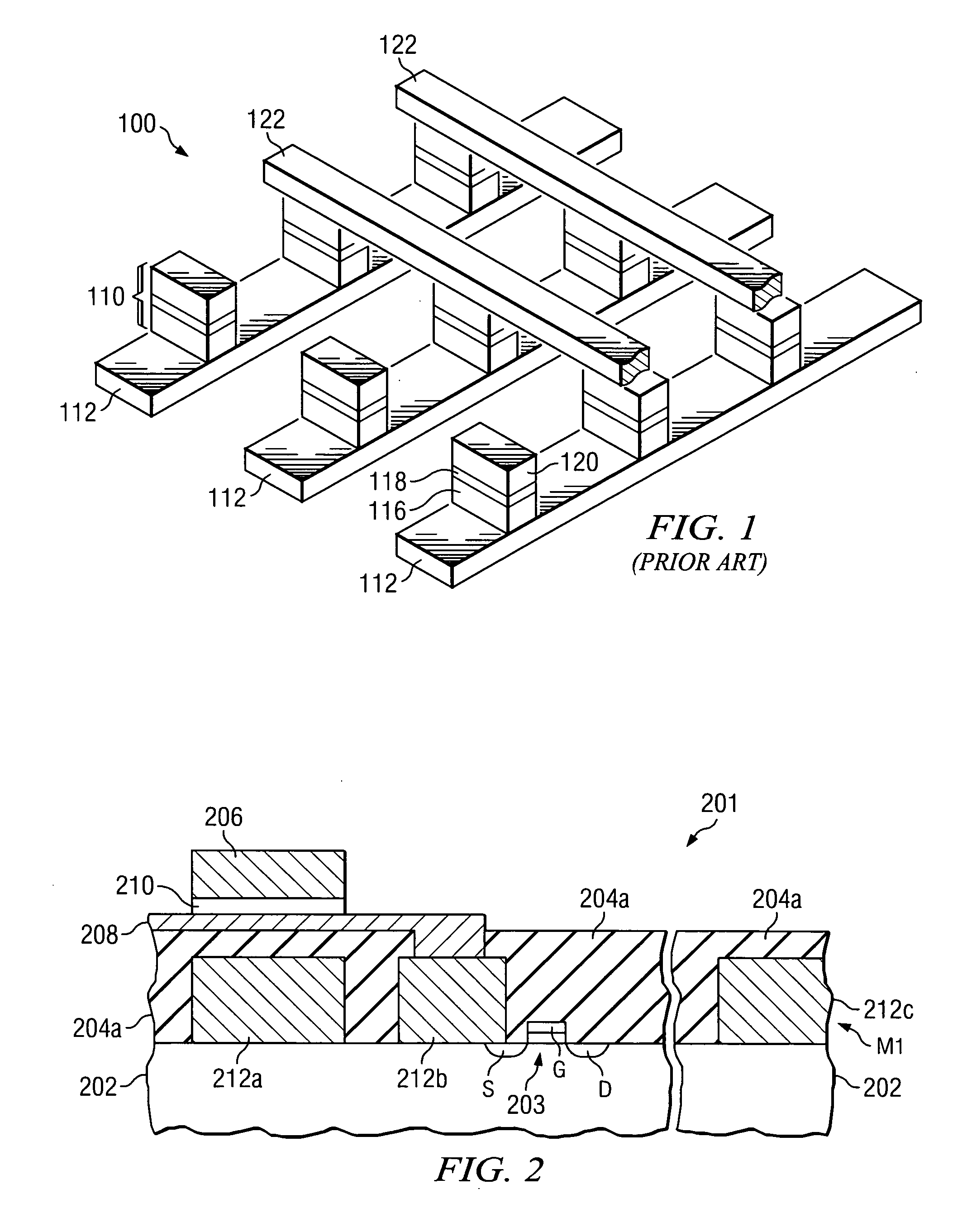
[0019]FIG. 1 illustrates a perspective view of a prior art cross-point MRAM array 100 having bitlines 122 located substantially perpend...


PUM


Abstract

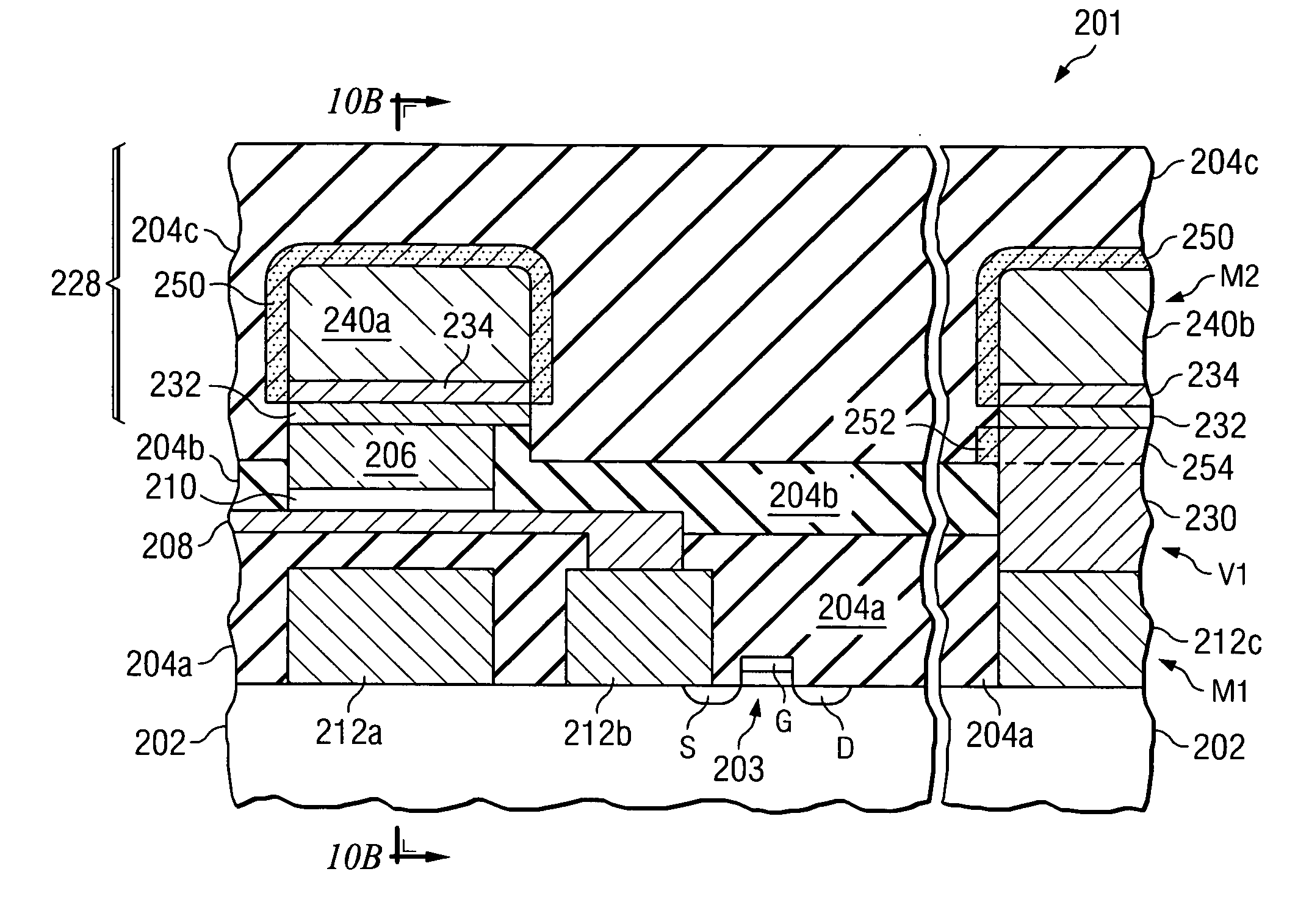
A method of forming a ferromagnetic liner on conductive lines of magnetic memory devices and a structure thereof. The ferromagnetic liner increases the flux concentration of current run through the conductive lines, reducing the amount of write current needed to switch magnetic memory cells. The conductive lines are formed in a plate-up method, and the ferromagnetic liner is selectively formed on the plated conductive lines. The ferromagnetic liner may also be formed over conductive lines and a top portion of vias in a peripheral region of the workpiece.

Description

CROSS-REFERENCE TO RELATED APPLICATIONS [0001] This application relates to the following co-pending and commonly assigned patent application: U.S. Ser. No. 10 / 249,528, filed on Apr. 17, 2003, entitled, “Magnetically Lined Conductors,” which application is hereby incorporated herein by reference.TECHNICAL FIELD [0002] The present invention relates generally to the fabrication of semiconductor devices, and more particularly to the fabrication of magnetic memory devices. BACKGROUND [0003] Semiconductors are used in integrated circuits for electronic applications, including radios, televisions, cell phones, and personal computing devices, as examples. One type of semiconductor device is a semiconductor storage device, such as a dynamic random access memory (DRAM) or flash memory, which use electric charge to store information. [0004] A recent development in semiconductor memory devices involves spin electronics, which combines semiconductor technology and magnetics. The spin of electron...

Claims


Application Information

Patent Timeline
Patent Type & Authority Applications(United States)
IPC IPC(8): H01L23/52H01L21/4763H10B99/00
CPCH01L21/76852H01L21/76873H01L43/12H01L21/76885H01L27/228H01L21/76874H10B61/22H10N50/01
Inventor LEUSCHNER, RAINERGAIDIS, MICHAEL C.RUBINO, JUDITH M.ROMANKIW, LUBOMYR TARAS
Owner INFINEON TECH AG
Learn More