
Semiconductor device having copper wiring and its manufacture method

a technology of semiconductor devices and manufacturing methods, applied in semiconductor devices, semiconductor/solid-state device details, electrical apparatus, etc., can solve the problems of unsatisfactory conventional cu wiring forming methods, inability to obtain sufficient stressmigration resistance, etc., and achieve sufficient stressmigration and enhanced electrical resistance

Active Publication Date: 2006-01-19
FUJITSU LTD
View PDF8 Cites 17 Cited by
  • Summary
  • Abstract
  • Description
  • Claims
  • Application Information

AI Technical Summary

Benefits of technology

[0012] By making a purity of copper in a conductive plug different from a purity of copper in a wiring, it is possible to obtain an electromigration resistance and a stressmigration resistance suitable for the conductive plug and wiring. By setting an impurity concentration of the conductive plug relatively low, the electromigration resistance can be enhanced. By setting an impurity concentration of the wiring relatively high, a sufficient stressmigration can be ensured.

Problems solved by technology

A conventional Cu wiring forming method is, however, unsatisfactory in that a sufficient stressmigration resistance cannot be obtained in some cases.

Method used


Image

  • Semiconductor device having copper wiring and its manufacture method
  • Semiconductor device having copper wiring and its manufacture method
  • Semiconductor device having copper wiring and its manufacture method

Examples


Embodiment Construction

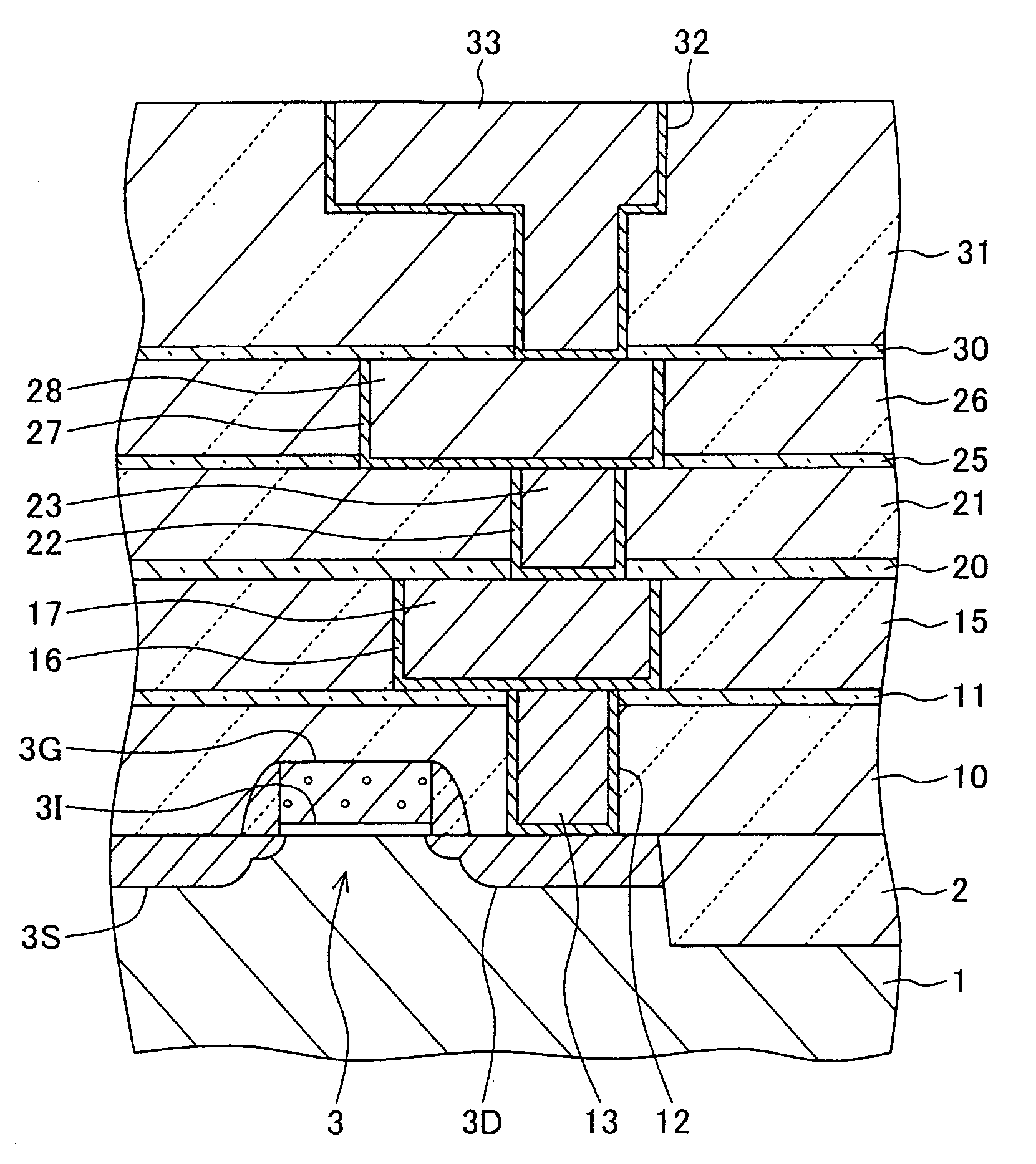
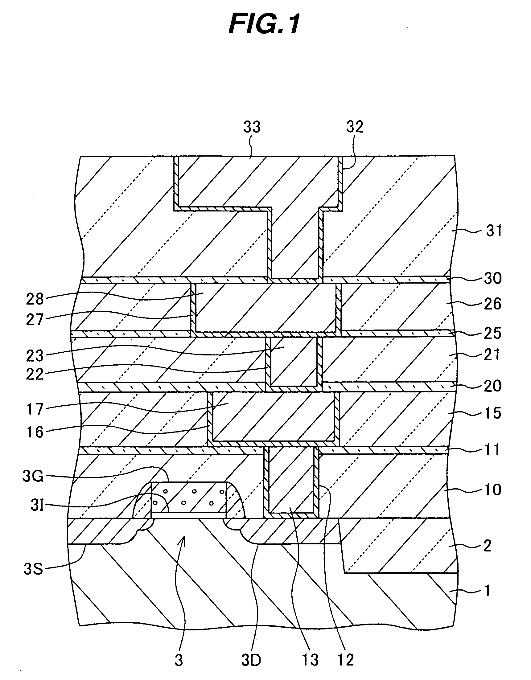
[0018]FIG. 1 is a cross sectional view of a semiconductor device according to the embodiment. In a surface layer of a semiconductor device 1 of silicon, an element isolation insulating film 2 of a shallow trench isolation (STI) structure is formed to define active regions. In an active region, a MOS transistor 3 is formed. The MOS transistor 3 is constituted of a source region 3S, a drain region 3D, a gate insulating film 31 and a gate electrode 3G.

[0019] An interlayer insulating film 10 of silicon oxide having a thickness of 300 nm and a protective film 11 of silicon carbide (SiC) having a thickness of 50 nm are formed on the semiconductor substrate 1, covering the MOS transistor 3. A via hole is formed through the protective film 11 and interlayer insulating film 10, exposing a partial surface of the drain region 3D on the bottom of the via hole. A conductive plug 13 of tungsten (W) is filled in the via hole. A barrier metal layer 12 of TiN having a thickness of 25 nm is disposed...


PUM

PropertyMeasurementUnit
thicknessaaaaaaaaaa
thicknessaaaaaaaaaa
thicknessaaaaaaaaaa

Abstract

A first interlayer insulating film made of insulting material is formed over an underlying substrate. A via hole is formed through the first interlayer insulating film. A conductive plug made of copper or alloy mainly consisting of copper is filled in the via hole. A second interlayer insulating film made of insulating material is formed over the first interlayer insulating film. A wiring groove is formed in the second interlayer insulating film, passing over the conductive plug and exposing the upper surface of the conductive plug. A wiring made of copper or alloy mainly consisting of copper is filled in the wiring groove. The total atom concentration of carbon, oxygen, nitrogen, sulfur and chlorine in the conductive plug is lower than the total atom concentration of carbon, oxygen, nitrogen, sulfur and chlorine in the wiring.

Description

CROSS REFERENCE TO RELATED APPLICATION [0001] This application is based on and claims priority of Japanese Patent Application No. 2004-207251 filed on Jul. 14, 2004, the entire contents of which are incorporated herein by reference. BACKGROUND OF THE INVENTION [0002] A) Field of the Invention [0003] The present invention relates to a semiconductor device having copper wirings and conductive plugs and its manufacture method. [0004] B) Description of the Related Art [0005] As LSI wiring material, copper (Cu) is now used which has a lower electric resistance and a higher electromigration resistance than aluminum (Al) used conventionally. A damascene method has generally been used for forming a Cu wiring, by which a Cu layer is deposited on an interlayer insulating film and filled in a recess formed in the film, and thereafter an unnecessary Cu layer is removed by chemical mechanical polishing (CMP). A single damascene method executes separately the process of filling a Cu layer in a vi...

Claims


Application Information

Patent Timeline
Patent Type & Authority Applications(United States)
IPC IPC(8): H01L23/52
CPCH01L21/2885H01L21/76877H01L23/53228H01L2924/0002H01L2924/00H01L21/3205
Inventor KOURA, YUMIKOKITADA, HIDEKI
Owner FUJITSU LTD
Learn More