Spin transistor, programmable logic circuit, and magnetic memory
a programmable logic and spin transistor technology, applied in the field of spin transistors, can solve the problems of reducing the response speed of devices, difficult to apply such spin transistors to logic circuits that include a number of devices, and the magnetic semiconductor cannot presently exhibit a preferable angle ratio at room temperatur
- Summary
- Abstract
- Description
- Claims
- Application Information
AI Technical Summary
Problems solved by technology
Method used
Image


Examples
first embodiment
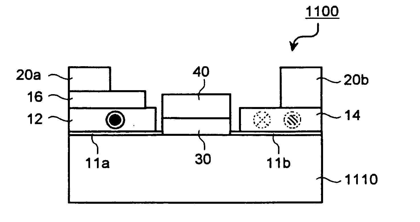
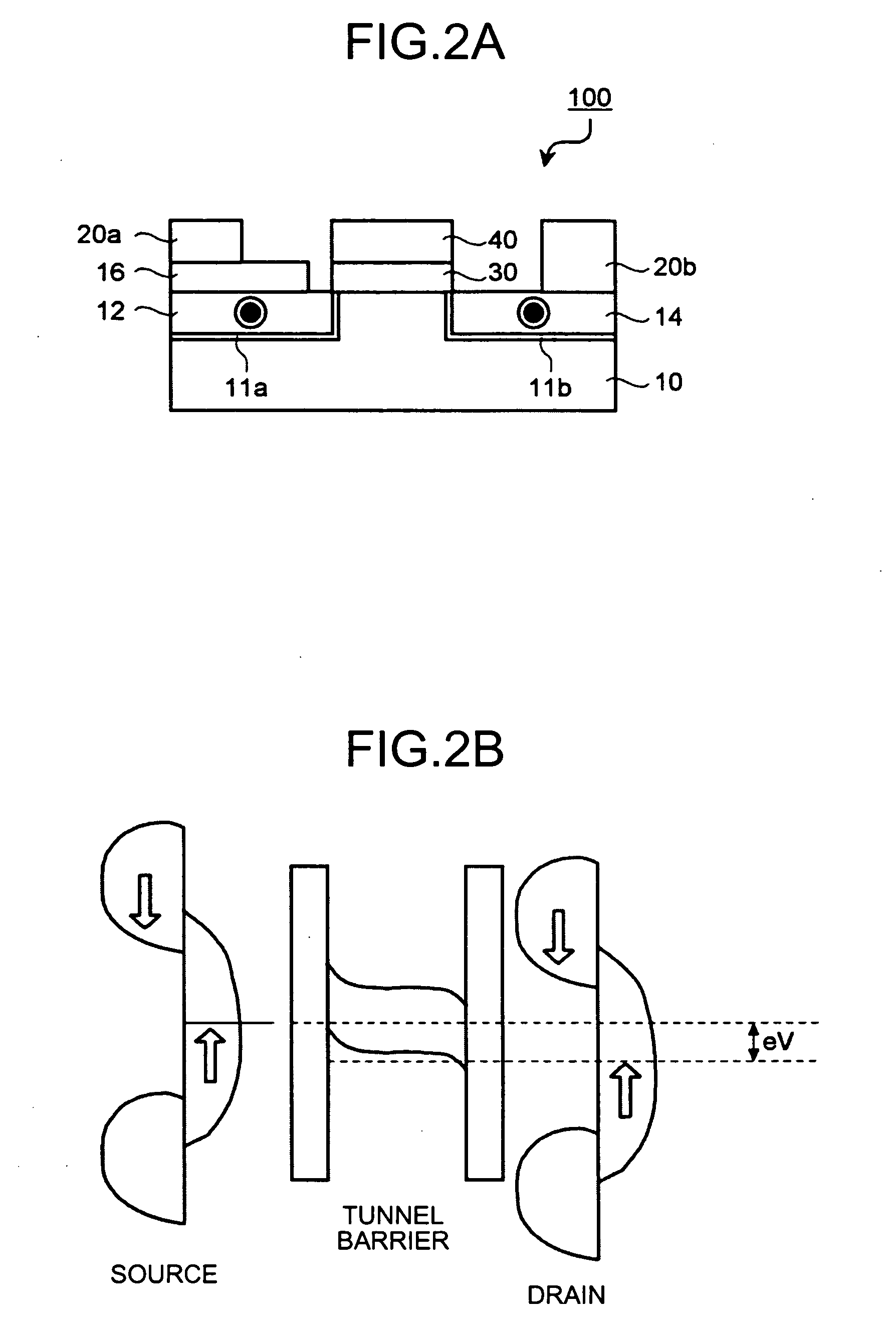
[0065] A spin transistor according to the present invention is a transistor with a MOS structure that has a source and a drain formed with a magnetic material. Also, such a spin transistor characteristically has a tunnel barrier film found between the channel and the source and / or the drain.
[0066]FIG. 1 is a schematic cross-sectional view of a spin transistor of the first embodiment. In FIG. 1, a spin transistor 100 includes a semiconductor substrate 10, a first conductive layer 12 and a second conductive layer 14 that are formed on the semiconductor substrate 10, a tunnel barrier film 11a that is formed between the first conductive layer 12 and the semiconductor substrate 10, a tunnel barrier film 11b that is formed between the second conductive layer 14 and the semiconductor substrate 10, a gate insulating film 30 that is formed on a part of the semiconductor substrate 10 that is located between the first conductive layer 12 and the second conductive layer 14, a gate electrode 40 ...
third embodiment
[0099] With the spin transistor 120 the magnetic cover layers 122a and 122b formed over the first word line 121a and the second word line 121b provide a current magnetic field locally to the second conductive layer 14. In other words, the necessary current pulse to control the magnetizing direction of the second conductive layer 14 can be made smaller. Thus, the problems that are caused by an increase in current pulse, such as EM (Electro Migration) and an increase in the area of a current pulse generating circuit, can be prevented.
[0100]FIG. 9 is a graph showing the drain current characteristics of a spin transistor according to the third embodiment. The first conductive layer 12 of the spin transistor used to prepare the graph is a ferromagnetic multi-layer film of (Co90Fe10)85B15 / PtMn / Ta / Poly-Si, while the second conductive layer 14 is a ferromagnetic multi-layer film of (Co90Fe10)85B15 / Ta / Poly-Si. In FIG. 9, the solid lines indicate the cases where the magnetizing direction of ...
fourth embodiment
[0114] Although in FIGS. 11A and 11B, the first multi-layer film and the second multi-layer film extend in parallel with each other in the longitudinal direction of the second conductive layer 14, it is possible to rotate the arrangement by 90 degrees and allow a gap between the top end of the first multi-layer film and the top end of the second multi-layer film. FIG. 13A is a schematic cross-sectional view of a spin transistor of this version of the FIG. 13B is a plan view of the spin transistor shown in FIG. 13A. A spin transistor 140 illustrated in FIG. 13A has a non-magnetic layer 141a and a magnetism fixing layer 142a stacked in this order on the surface of the second conductive layer 14 as the first multi-layer film. The spin transistor 140 also has a non-magnetic layer (not shown) and a magnetism fixing layer 142b stacked in this order on the surface of the second conductive layer 14 as the second multi-layer film. Particularly, the first multi-layer film and the second mult...
PUM
 Abstract
Description
Claims
Application Information
 - R&D
- Intellectual Property
- Life Sciences
- Materials
- Tech Scout
- Unparalleled Data Quality
- Higher Quality Content
- 60% Fewer Hallucinations
Browse by: Latest US Patents, China's latest patents, Technical Efficacy Thesaurus, Application Domain, Technology Topic, Popular Technical Reports.
© 2025 PatSnap. All rights reserved.Legal|Privacy policy|Modern Slavery Act Transparency Statement|Sitemap|About US| Contact US: help@patsnap.com