Liquid crystal display driver device and liquid crystal display system
a driver device and liquid crystal display technology, applied in the direction of instruments, computing, electric digital data processing, etc., can solve the problems of display image quality deterioration risk, achieve high-quality display, avoid display image quality degradation, and reduce emi
- Summary
- Abstract
- Description
- Claims
- Application Information
AI Technical Summary
Benefits of technology
Problems solved by technology
Method used
Image
Examples
first embodiment
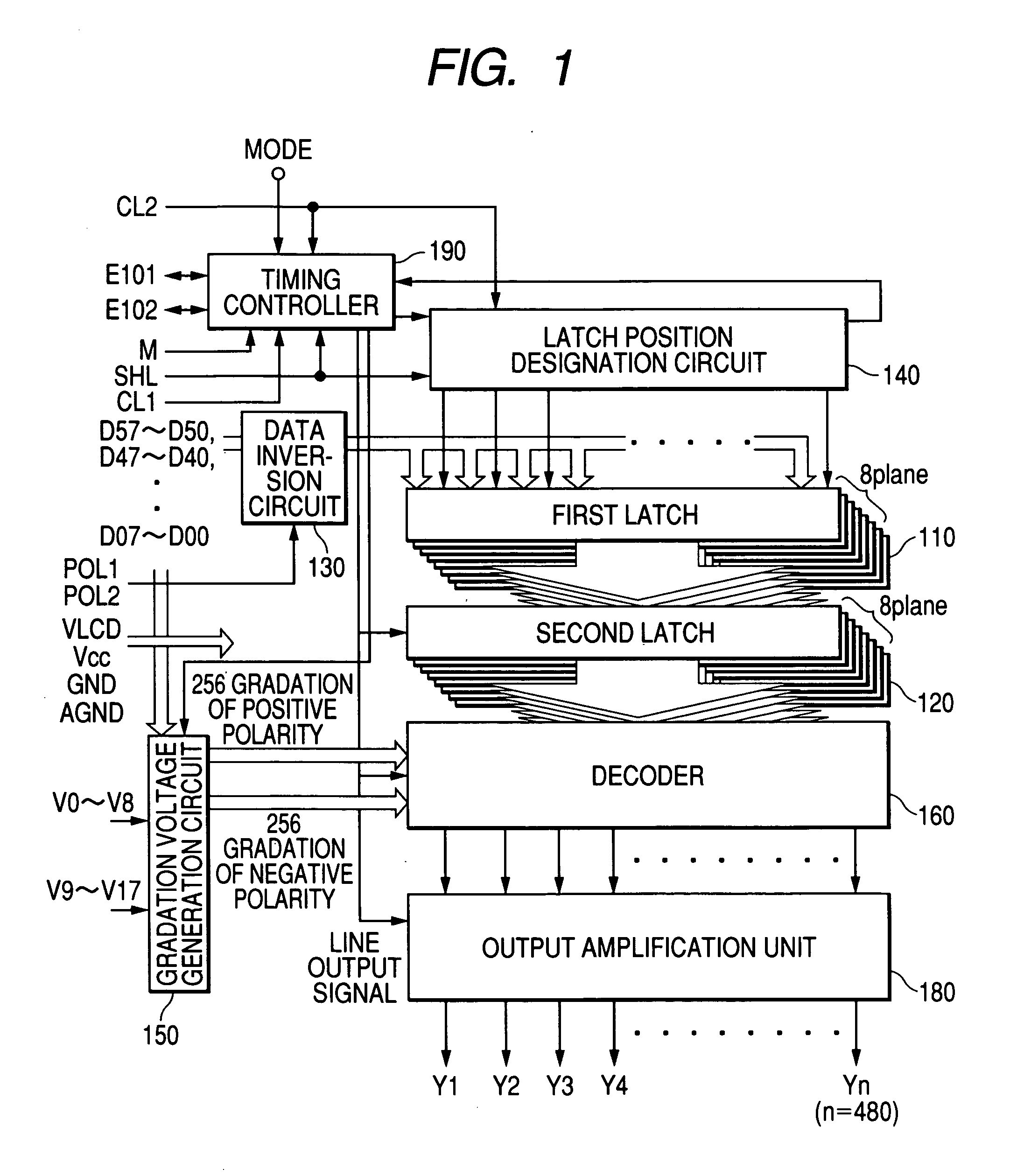
[0053]FIG. 3 is a block diagram with the output amplification unit 180, and the timing controller 190, partially cut away from the liquid crystal display driver shown in FIG., 1, showing the configuration thereof, as a feature of the invention.
[0054] As shown in FIG. 3, the present embodiment is provided with a delay circuit 191 for delaying the line output signal LOC1 by predetermined time Td, a signal path switchover circuit 193 capable of passing the delayed line signal LOC2, and the line output signal LOC1 before being delayed, causing both the signals to intersect each other, and switching over therebetween, and a signal generation circuit 192 comprising a D-type bistable trigger circuit FF1 for generating a switchover control signal PCS for executing switchover in the signal path switchover circuit 193, based on the AC conversion signal M. The optimum value of the delay time Td in the delay circuit 191 is on the order of 0.1 μs (microsecond), that is, a value equivalent to abo...
second embodiment
[0075]FIG. 9 shows the invention. With the present embodiment, a plurality of delay circuits DLY1, DLY2 . . . DLYm, for delaying a line output signal LOC0 differing in delay time from each other, are provided to generate the line output signals LOC0, LOC1 to LOCm, each differing in timing, while the n pieces of the output amplifiers of the output amplification unit 180 are divided into (m+1) pieces of groups, and the line output signals LOC0 to LOCm are changed over in the signal path switchover circuit 193 for every suitable period (for example, a period m times the period of the AC conversion signal M) before being sequentially fed into the output amplifiers of the respective groups, thereby executing operation at different timings. The present embodiment is advantageous in that the peak of current flowing through the source lines of the liquid crystal panel can be further lowered.
[0076] In FIG. 9, there is described the embodiment wherein the n pieces of the output amplifiers of ...
PUM
| Property | Measurement | Unit |
|---|---|---|
| voltage | aaaaa | aaaaa |
| display time | aaaaa | aaaaa |
| outputting voltages | aaaaa | aaaaa |
Abstract
Description
Claims
Application Information
 - R&D
- Intellectual Property
- Life Sciences
- Materials
- Tech Scout
- Unparalleled Data Quality
- Higher Quality Content
- 60% Fewer Hallucinations
Browse by: Latest US Patents, China's latest patents, Technical Efficacy Thesaurus, Application Domain, Technology Topic, Popular Technical Reports.
© 2025 PatSnap. All rights reserved.Legal|Privacy policy|Modern Slavery Act Transparency Statement|Sitemap|About US| Contact US: help@patsnap.com


